CY8C24123A CY8C24223A CY8C24423A PSoC® Programmable System-on-Chip PSoC® Programmable System-on-Chip Features ■ ■ ■ ■ ■ Powerful Harvard-architecture processor ❐ M8C processor speeds up to 24 MHz ❐ 8 × 8 multiply, 32-bit accumulate ❐ Low power at high speed ❐ Operating voltage: 2.4 V to 5.25 V ❐ Operating voltages down to 1.
CY8C24123A CY8C24223A CY8C24423A Contents PSoC Functional Overview .............................................. 3 PSoC Core .................................................................. 3 Digital System ............................................................. 3 Analog System ............................................................ 4 Additional System Resources ..................................... 5 PSoC Device Characteristics ...................................... 5 Getting Started ........
CY8C24123A CY8C24223A CY8C24423A PSoC Functional Overview Digital System The digital system consists of four digital PSoC blocks. Each block is an 8-bit resource that may be used alone or combined with other blocks to form 8-, 16-, 24-, and 32-bit peripherals, which are called user module references. Figure 1. Digital System Block Diagram Port 1 Port 2 The PSoC architecture, shown in Figure 1, consists of four main areas: PSoC core, digital system, analog system, and system resources.
CY8C24123A CY8C24223A CY8C24423A The analog system consists of six configurable blocks, each consisting of an opamp circuit that allows the creation of complex analog signal flows. Analog peripherals are very flexible and can be customized to support specific application requirements. Some of the more common PSoC analog functions (most available as user modules) are: ■ ■ ADCs (up to two, with 6- to 14-bit resolution, selectable as incremental, delta sigma, and SAR) Figure 2.
CY8C24123A CY8C24223A CY8C24423A Additional System Resources System resources, some of which are listed in the previous sections, provide additional capability useful to complete systems. Additional resources include a multiplier, decimator, switch-mode pump, low-voltage detection, and power-on-reset (POR). Statements describing the merits of each system resource follow: ■ Digital clock dividers provide three customizable clock frequencies for use in applications.
CY8C24123A CY8C24223A CY8C24423A Getting Started For in depth information, along with detailed programming details, see the PSoC® Technical Reference Manual. CYPros Consultants For up-to-date ordering, packaging, and electrical specification information, see the latest PSoC device datasheets on the web. Certified PSoC Consultants offer everything from technical assistance to completed PSoC designs. To contact or become a PSoC Consultant go to the CYPros Consultants web site.
CY8C24123A CY8C24223A CY8C24423A Debugger In-Circuit Emulator PSoC Designer has a debug environment that provides hardware in-circuit emulation, allowing you to test the program in a physical system while providing an internal view of the PSoC device. Debugger commands allow you to read and program and read and write data memory, and read and write I/O registers. You can read and write CPU registers, set and clear breakpoints, and provide program run, halt, and step control.
CY8C24123A CY8C24223A CY8C24423A Pinouts This section describes, lists, and illustrates the CY8C24x23A PSoC device pins and pinout configurations. Every port pin (labeled with a “P”) is capable of digital I/O. However, VSS, VDD, SMP, and XRES are not capable of digital I/O. 8-Pin Part Pinout Table 2. 8-Pin PDIP and SOIC Pin No.
CY8C24123A CY8C24223A CY8C24423A 20-Pin Part Pinout Table 3. 20-Pin PDIP, SSOP, and SOIC Pin No.
CY8C24123A CY8C24223A CY8C24423A 28-Pin Part Pinout Table 4. 28-Pin PDIP, SSOP, and SOIC Pin No.
CY8C24123A CY8C24223A CY8C24423A 32-Pin Part Pinout Table 5.
CY8C24123A CY8C24223A CY8C24423A 56-Pin Part Pinout The 56-pin SSOP part is for the CY8C24000A On-Chip Debug (OCD) PSoC device. Note This part is only used for in-circuit debugging. It is NOT available for production. Table 6. 56-Pin SSOP OCD Pin No. 1 2 3 4 5 6 7 8 9 10 11 12 13 14 15 16 Type Digital Analog I/O I/O I/O I/O I/O I/O I/O I/O I I I I OCD OCD Power I I Pin Name NC P0[7] P0[5] P0[3] P0[1] P2[7] P2[5] P2[3] P2[1] NC NC NC NC OCDE OCDO SMP Description No connection.
CY8C24123A CY8C24223A CY8C24423A Register Reference This section lists the registers of the CY8C24x23A PSoC device. For detailed register information, see the PSoC Programmable Sytem-on-Chip Reference Manual. Register Conventions Register Mapping Tables Abbreviations Used The PSoC device has a total register address space of 512 bytes. The register space is referred to as I/O space and is divided into two banks, Bank 0 and Bank 1.
CY8C24123A CY8C24223A CY8C24423A Table 8.
CY8C24123A CY8C24223A CY8C24423A Table 0-1.
CY8C24123A CY8C24223A CY8C24423A Electrical Specifications This section presents the DC and AC electrical specifications of the CY8C24x23A PSoC device. For the latest electrical specifications, check if you have the most recent datasheet by visiting the website at http://www.cypress.com. Specifications are valid for –40 °C TA 85 °C and TJ 100 °C, except where noted. Refer to Table 29 on page 34 for the electrical specifications for the IMO using SLIMO mode. Figure 8.
CY8C24123A CY8C24223A CY8C24423A Operating Temperature Table 10. Operating Temperature Symbol Description TA Ambient temperature TJ Junction temperature Min –40 –40 Typ – – Max +85 +100 Units Notes °C °C The temperature rise from ambient to junction is package specific. See Table 48 on page 53.
CY8C24123A CY8C24223A CY8C24423A DC GPIO Specifications The following tables list the guaranteed maximum and minimum specifications for the voltage and temperature ranges: 4.75 V to 5.25 V and –40 °C TA 85 °C, 3.0 V to 3.6 V and –40 °C TA 85 °C, or 2.4 V to 3.0 V and –40 °C TA 85 °C, respectively. Typical parameters are measured at 5 V, 3.3 V, and 2.7 V at 25 °C and are for design guidance only. Table 12. 5-V and 3.
CY8C24123A CY8C24223A CY8C24423A DC Operational Amplifier Specifications The following tables list the guaranteed maximum and minimum specifications for the voltage and temperature ranges: 4.75 V to 5.25 V and –40 °C TA 85 °C, 3.0 V to 3.6 V and –40 °C TA 85 °C, or 2.4 V to 3.0 V and –40 °C TA 85 °C, respectively. Typical parameters are measured at 5 V, 3.3 V, and 2.7 V at 25 °C and are for design guidance only.
CY8C24123A CY8C24223A CY8C24423A Table 15. 3.3-V DC Operational Amplifier Specifications Symbol Description Min Typ Max Units VOSOA Input offset voltage (absolute value) Power = low, Opamp bias = high Power = medium, Opamp bias = high Power = high, Opamp bias = high – – – 1.65 1.32 – 10 8 – mV mV mV Notes Power = high, Opamp bias = high setting is not allowed for 3.3 V VDD operation. TCVOSOA Average input offset voltage drift – 7.0 35.
CY8C24123A CY8C24223A CY8C24423A Table 16. 2.7-V DC Operational Amplifier Specifications Symbol Description Min Typ Max Units VOSOA Input offset voltage (absolute value) Power = low, Opamp bias = high Power = medium, Opamp bias = high Power = high, Opamp bias = high – – – 1.65 1.32 – 10 8 – mV mV mV Notes Power = high, Opamp bias = high setting is not allowed for 2.7 V VDD operation. TCVOSOA Average input offset voltage drift – 7.0 35.
CY8C24123A CY8C24223A CY8C24423A DC Analog Output Buffer Specifications The following tables list the guaranteed maximum and minimum specifications for the voltage and temperature ranges: 4.75 V to 5.25 V and –40 °C TA 85 °C, 3.0 V to 3.6 V and –40 °C TA 85 °C, or 2.4 V to 3.0 V and –40 °C TA 85 °C, respectively. Typical parameters are measured at 5 V, 3.3 V, and 2.7 V at 25 °C and are for design guidance only. Table 18.
CY8C24123A CY8C24223A CY8C24423A Table 20. 2.7-V DC Analog Output Buffer Specifications Min Typ Max Units Notes CL Symbol Load Capacitance – – 200 pF This specification applies to the external circuit that is being driven by the analog output buffer.
CY8C24123A CY8C24223A CY8C24423A Table 21. DC Switch Mode Pump (SMP) Specifications (continued) Symbol Description Min Typ Max Units Notes 1.2 – – V Configuration listed in footnote.[10] 0 °C TA 100. 1.25 V at TA = –40 °C VBATSTART Minimum input voltage from battery to start pump VPUMP_Line Line regulation (over VBAT range) – 5 – %VO Configuration listed in footnote.
CY8C24123A CY8C24223A CY8C24423A DC Analog Reference Specifications The following tables list the guaranteed maximum and minimum specifications for the voltage and temperature ranges: 4.75 V to 5.25 V and –40 °C TA 85 °C, 3.0 V to 3.6 V and –40 °C TA 85 °C, or 2.4 V to 3.0 V and –40 °C TA 85 °C, respectively. Typical parameters are measured at 5 V, 3.3 V, and 2.7 V at 25 °C and are for design guidance only.
CY8C24123A CY8C24223A CY8C24423A Table 22.
CY8C24123A CY8C24223A CY8C24423A Table 22.
CY8C24123A CY8C24223A CY8C24423A Table 23. 3.
CY8C24123A CY8C24223A CY8C24423A Table 23. 3.3-V DC Analog Reference Specifications (continued) Reference ARF_CR [5:3] Reference Power Settings Symbol Reference Description Typ Max Units – – – – P2[4] + 1.211 P2[4] + 1.285 P2[4] + 1.348 V P2[4] P2[4] P2[4] – 0b100 All power settings Not allowed at 3.3 V – – 0b101 RefPower = high Opamp bias = high VREFHI Ref High VAGND AGND VREFLO Ref Low P2[4] – Bandgap (P2[4] = VDD/2) P2[4] – 1.354 P2[4] – 1.290 P2[4] – 1.
CY8C24123A CY8C24223A CY8C24423A Table 24. 2.7-V DC Analog Reference Specifications Reference ARF_CR [5:3] Reference Power Settings Symbol Reference 0b000 All power settings Not allowed at 2.
CY8C24123A CY8C24223A CY8C24423A Table 24. 2.7-V DC Analog Reference Specifications (continued) (continued) Reference ARF_CR [5:3] Reference Power Settings Symbol Reference Description Min Typ Max Units 0b011 All power settings Not allowed at 2.7 V – – – – – – – 0b100 All power settings Not allowed at 2.7 V – – – – – – – 0b101 All power settings Not allowed at 2.
CY8C24123A CY8C24223A CY8C24423A DC POR, SMP, and LVD Specifications Table 23 lists the guaranteed maximum and minimum specifications for the voltage and temperature ranges: 4.75 V to 5.25 V and –40 °C TA 85 °C, 3.0 V to 3.6 V and –40 °C TA 85 °C, or 2.4 V to 3.0 V and –40 °C TA 85 °C, respectively. Typical parameters are measured at 5 V, 3.3 V, and 2.7 V at 25 °C and are for design guidance only. Note The bits PORLEV and VM in the following table refer to bits in the VLT_CR register.
CY8C24123A CY8C24223A CY8C24423A DC Programming Specifications Table 27 lists the guaranteed maximum and minimum specifications for the voltage and temperature ranges: 4.75 V to 5.25 V and –40 °C TA 85 °C, 3.0 V to 3.6 V and –40 °C TA 85 °C, or 2.4 V to 3.0 V and –40 °C TA 85 °C, respectively. Typical parameters are measured at 5 V, 3.3 V, and 2.7 V at 25 °C and are for design guidance only. Table 27. DC Programming Specifications Symbol VDDP Description VDD for programming and erase Min 4.
CY8C24123A CY8C24223A CY8C24423A AC Electrical Characteristics AC Chip-Level Specifications These tables list the guaranteed maximum and minimum specifications for the voltage and temperature ranges: 4.75 V to 5.25 V and –40 °C TA 85 °C, 3.0 V to 3.6 V and –40 °C TA 85 °C, or 2.4 V to 3.0 V and –40 °C TA 85 °C, respectively. Typical parameters are measured at 5 V, 3.3 V, and 2.7 V at 25 °C and are for design guidance only. Table 29. 5-V and 3.
CY8C24123A CY8C24223A CY8C24423A Table 29. 5-V and 3.
CY8C24123A CY8C24223A CY8C24423A Figure 10. PLL Lock Timing Diagram PLL Enable TPLLSLEW 24 MHz FPLL PLL Gain 0 Figure 11. PLL Lock for Low Gain Setting Timing Diagram PLL Enable TPLLSLEWLOW 24 MHz FPLL PLL Gain 1 Figure 12. External Crystal Oscillator Startup Timing Diagram 32K Select 32 kHz TOS F32K2 Document Number: 38-12028 Rev.
CY8C24123A CY8C24223A CY8C24423A AC GPIO Specifications These tables list the guaranteed maximum and minimum specifications for the voltage and temperature ranges: 4.75 V to 5.25 V and –40 °C TA 85 °C, 3.0 V to 3.6 V and –40 °C TA 85 °C, or 2.4 V to 3.0 V and –40 °C TA 85 °C, respectively. Typical parameters are measured at 5 V, 3.3 V, and 2.7 V at 25 °C and are for design guidance only. Table 31. 5-V and 3.
CY8C24123A CY8C24223A CY8C24423A AC Operational Amplifier Specifications The following tables list the guaranteed maximum and minimum specifications for the voltage and temperature ranges: 4.75 V to 5.25 V and –40 °C TA 85 °C, 3.0 V to 3.6 V and –40 °C TA 85 °C, or 2.4 V to 3.0 V and –40 °C TA 85 °C, respectively. Typical parameters are measured at 5 V, 3.3 V, and 2.7 V at 25 °C and are for design guidance only.
CY8C24123A CY8C24223A CY8C24423A Table 35. 2.7-V AC Operational Amplifier Specifications Symbol tROA tSOA Min Typ Max Units Rising settling time from 80% of V to 0.1% of V (10 pF load, unity gain) Power = low, Opamp bias = low Power = medium, Opamp bias = high Description – – – – 3.92 0.72 µs µs Falling settling time from 20% of V to 0.1% of V (10 pF load, unity gain) Power = low, Opamp bias = low Power = medium, Opamp bias = high – – – – 5.41 0.
CY8C24123A CY8C24223A CY8C24423A Figure 14. Typical Opamp Noise nV/rtHz 10000 PH_BH PH_BL PM_BL PL_BL 1000 100 10 0.001 0.01 0.1 Freq (kHz) 1 10 100 AC Low Power Comparator Specifications Table 36 lists the guaranteed maximum and minimum specifications for the voltage and temperature ranges: 4.75 V to 5.25 V and –40 °C TA 85 °C, 3.0 V to 3.6 V and –40 °C TA 85 °C, or 2.4 V to 3.0 V and –40 °C TA 85 °C, respectively.
CY8C24123A CY8C24223A CY8C24423A AC Digital Block Specifications The following tables list the guaranteed maximum and minimum specifications for the voltage and temperature ranges: 4.75 V to 5.25 V and –40 °C TA 85 °C, 3.0 V to 3.6 V and –40 °C TA 85 °C, or 2.4 V to 3.0 V and –40 °C TA 85 °C, respectively. Typical parameters are measured at 5 V, 3.3 V, and 2.7 V at 25 °C and are for design guidance only. Table 37. 5-V and 3.
CY8C24123A CY8C24223A CY8C24423A Table 38. 2.7-V AC Digital Block Specifications Function Description All Functions Block input clock frequency Timer Capture pulse width Input clock frequency, with or without capture Counter Dead Band Min Typ Max Units Notes – – 12.7 MHz 2.4 V < VDD < 3.0 V 100[26] – – ns – – 12.7 MHz 100[26] – – ns Input clock frequency, no enable input – – 12.7 MHz Input clock frequency, enable input – – 12.
CY8C24123A CY8C24223A CY8C24423A AC Analog Output Buffer Specifications The following tables list the guaranteed maximum and minimum specifications for the voltage and temperature ranges: 4.75 V to 5.25 V and –40 °C TA 85 °C, 3.0 V to 3.6 V and –40 °C TA 85 °C, or 2.4 V to 3.0 V and –40 °C TA 85 °C, respectively. Typical parameters are measured at 5 V, 3.3 V, and 2.7 V at 25 °C and are for design guidance only. Table 39.
CY8C24123A CY8C24223A CY8C24423A Table 41. 2.7-V AC Analog Output Buffer Specifications Min Typ Max Units tROB Symbol Rising settling time to 0.1%, 1 V Step, 100 pF load Power = low Power = high Description – – – – 4 4 µs µs tSOB Falling settling time to 0.1%, 1 V Step, 100 pF load Power = low Power = high – – – – 3 3 µs µs SRROB Rising slew rate (20% to 80%), 1 V Step, 100 pF load Power = low Power = high 0.4 0.
CY8C24123A CY8C24223A CY8C24423A Table 44. 2.7-V AC External Clock Specifications Min Typ Max Units FOSCEXT Symbol Frequency with CPU clock divide by 1[29] Description 0.093 – 12.3 MHz FOSCEXT Frequency with CPU clock divide by 2 or greater[30] 0.186 – 12.3 MHz ns – High period with CPU clock divide by 1 41.7 – 5300 – Low period with CPU clock divide by 1 41.
CY8C24123A CY8C24223A CY8C24423A AC I2C Specifications The following tables list the guaranteed maximum and minimum specifications for the voltage and temperature ranges: 4.75 V to 5.25 V and –40 °C TA 85 °C, 3.0 V to 3.6 V and –40 °C TA 85 °C, or 2.4 V to 3.0 V and –40 °C TA 85 °C, respectively. Typical parameters are measured at 5 V, 3.3 V, and 2.7 V at 25 °C and are for design guidance only. Table 46. AC Characteristics of the I2C SDA and SCL Pins for VDD > 3.
CY8C24123A CY8C24223A CY8C24423A Packaging Information This section illustrates the packaging specifications for the CY8C24x23A PSoC device, along with the thermal impedances for each package and the typical package capacitance on crystal pins. Important Note Emulation tools may require a larger area on the target PCB than the chip's footprint. For a detailed description of the emulation tools' dimensions, see the emulator pod drawings at http://www.cypress.com/design/MR10161.
CY8C24123A CY8C24223A CY8C24423A Figure 17. 8-Pin (150-Mil) SOIC 51-85066 *E Figure 18. 20-Pin (300-Mil) Molded DIP 51-85011 *C Document Number: 38-12028 Rev.
CY8C24123A CY8C24223A CY8C24423A Figure 19. 20-Pin (210-Mil) SSOP 51-85077 *E Document Number: 38-12028 Rev.
CY8C24123A CY8C24223A CY8C24423A Figure 20. 20-Pin (300-Mil) Molded SOIC 51-85024 *E Figure 21. 28-Pin (300-Mil) Molded DIP 51-85014 *F Document Number: 38-12028 Rev.
CY8C24123A CY8C24223A CY8C24423A Figure 22. 28-Pin (210-Mil) SSOP 51-85079 *E Figure 23. 28-Pin (300-Mil) Molded SOIC 51-85026 *F Document Number: 38-12028 Rev.
CY8C24123A CY8C24223A CY8C24423A Figure 24. 32-Pin Sawn QFN Package 001-30999 *C Important Note For information on the preferred dimensions for mounting QFN packages, see the application note, Application Notes for Surface Mount Assembly of Amkor's MicroLeadFrame (MLF) Packages available at http://www.amkor.com. Figure 25. 56-Pin (300-Mil) SSOP 51-85062 *E Document Number: 38-12028 Rev.
CY8C24123A CY8C24223A CY8C24423A Thermal Impedances Capacitance on Crystal Pins Table 48. Thermal Impedances per Package Package Typical JA Table 49. Typical Package Capacitance on Crystal Pins [33] Package Package Capacitance 8-pin PDIP 123 °C/W 8-pin PDIP 2.8 pF 8-pin SOIC 185 °C/W 8-pin SOIC 2.0 pF 20-pin PDIP 109 °C/W 20-pin PDIP 3.0 pF 20-pin SSOP 117 °C/W 20-pin SSOP 2.6 pF 20-pin SOIC 81 °C/W 20-pin SOIC 2.5 pF 28-pin PDIP 69 °C/W 28-pin PDIP 3.
CY8C24123A CY8C24223A CY8C24423A Development Tool Selection This section presents the development tools available for all current PSoC device families including the CY8C24x23A family. Software PSoC Designer CY3210-MiniProg1 The CY3210-MiniProg1 kit lets you to program PSoC devices through the MiniProg1 programming unit. The MiniProg is a small, compact prototyping programmer that connects to the PC through a provided USB 2.0 cable.
CY8C24123A CY8C24223A CY8C24423A Device Programmers All device programmers can be purchased from the Cypress Online Store. CY3216 Modular Programmer The CY3216 Modular Programmer kit features a modular programmer and the MiniProg1 programming unit. The modular programmer includes three programming module cards and supports multiple Cypress products.
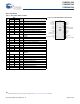
CY8C24123A CY8C24223A CY8C24423A Ordering Information CY8C24423A-24SXI CY8C24423A-24SXIT CY8C24423A-24LTXI CY8C24423A-24LTXIT CY8C24000A-24PVXI[38] XRES Pin CY8C24423A-24PVXIT Analog Outputs CY8C24423A-24PXI CY8C24423A-24PVXI Analog Inputs CY8C24223A-24SXIT Digital I/O Pins CY8C24223A-24SXI Analog Blocks CY8C24223A-24PVXIT Digital Blocks CY8C24223A-24PXI CY8C24223A-24PVXI Temperature Range CY8C24123A-24SXIT Switch Mode Pump CY8C24123A-24PXI CY8C24123A-24SXI SRAM (Bytes) 8-pin (300-mil) DI
CY8C24123A CY8C24223A CY8C24423A Acronyms Acronyms Used Table 53 lists the acronyms that are used in this document. Table 53.
CY8C24123A CY8C24223A CY8C24423A Document Conventions Units of Measure Table 54 lists the unit sof measures. Table 54.
CY8C24123A CY8C24223A CY8C24423A Glossary (continued) bandwidth 1. The frequency range of a message or information processing system measured in hertz. 2. The width of the spectral region over which an amplifier (or absorber) has substantial gain (or loss); it is sometimes represented more specifically as, for example, full width at half maximum. bias 1. A systematic deviation of a value from a reference value. 2. The amount by which the average of a set of values departs from a reference value. 3.
CY8C24123A CY8C24223A CY8C24423A Glossary (continued) digital blocks The 8-bit logic blocks that can act as a counter, timer, serial receiver, serial transmitter, CRC generator, pseudo-random number generator, or SPI. digital-to-analog (DAC) A device that changes a digital signal to an analog signal of corresponding magnitude. The analogto-digital (ADC) converter performs the reverse operation. duty cycle The relationship of a clock period high time to its low time, expressed as a percent.
CY8C24123A CY8C24223A CY8C24423A Glossary (continued) M8C An 8-bit Harvard-architecture microprocessor. The microprocessor coordinates all activity inside a PSoC by interfacing to the Flash, SRAM, and register space. master device A device that controls the timing for data exchanges between two devices. Or when devices are cascaded in width, the master device is the one that controls the timing for data exchanges between the cascaded devices and an external interface.
CY8C24123A CY8C24223A CY8C24423A Glossary (continued) ROM An acronym for read only memory. A data-storage device from which data can be read out, but new data cannot be written in. serial 1. Pertaining to a process in which all events occur one after the other. 2. Pertaining to the sequential or consecutive occurrence of two or more related activities in a single device or channel.
CY8C24123A CY8C24223A CY8C24423A Document History Page Document Title: CY8C24123A, CY8C24223A, CY8C24423A PSoC® Programmable System-on-Chip Document Number: 38-12028 Revision ECN Orig. of Change Submission Date ** 236409 SFV See ECN New silicon and new document – Preliminary datasheet. *A 247589 SFV See ECN Changed the title to read “Final” datasheet. Updated Electrical Specifications chapter. Description of Change *B 261711 HMT See ECN Input all SFV memo changes.
CY8C24123A CY8C24223A CY8C24423A Document Title: CY8C24123A, CY8C24223A, CY8C24423A PSoC® Programmable System-on-Chip Document Number: 38-12028 Revision ECN Orig. of Change Submission Date *L 2897881 MAXK/NJF *M 2942375 VMAD *N 3032514 NJF *O 3098766 YJI 12/01/2010 Sunset review; no content update *P 3351721 YJI 08/31/2011 Full annual review of document. No changes are required.
CY8C24123A CY8C24223A CY8C24423A Sales, Solutions, and Legal Information Worldwide Sales and Design Support Cypress maintains a worldwide network of offices, solution centers, manufacturers’ representatives, and distributors. To find the office closest to you, visit us at Cypress Locations. Products Automotive Clocks & Buffers Interface Lighting & Power Control PSoC Solutions cypress.com/go/automotive cypress.com/go/clocks psoc.cypress.com/solutions cypress.