
Programmable System-on-Chip Specification Sheet


CY8C24223A, CY8C24423A
Document Number: 3-12029 Rev. *E Page 16 of 31
DC Electrical Characteristics
DC Chip-Level Specifications
The following table lists guaranteed maximum and minimum specifications for the voltage and temperature ranges: 4.75V to 5.25V
and -40°C ≤ T
A
≤ 125°C. Typical parameters apply to 5V at 25°C and are for design guidance only.
DC General Purpose IO Specifications
The following tables list guaranteed maximum and minimum specifications for the voltage and temperature ranges: 4.75V to 5.25V
and -40°C ≤ T
A
≤ 125°C. Typical parameters apply to 5V at 25°C and are for design guidance.
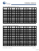
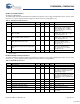
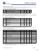
Table 11. DC Chip-Level Specifications
Symbol Description Min Typ Max Units Notes
Vdd Supply Voltage 4.75 – 5.25 V
I
DD
Supply Current – 5 8 mA Conditions are Vdd = 5.25V, -40
o
C ≤ T
A
≤ 125
o
C, CPU = 3 MHz, SYSCLK
doubler disabled, VC1 = 1.5 MHz,
VC2 = 93.75 kHz, VC3 = 93.75 kHz,
analog power = off.
I
SB
Sleep (Mode) Current with POR, LVD, Sleep
Timer, and WDT.
a
a. Standby current includes all functions (POR, LVD, WDT, Sleep Time) needed for reliable system operation. This must be compared with devices that have similar
functions enabled.
– 4 13 μA Conditions are with internal slow speed
oscillator, Vdd = 5.25V, -40
o
C ≤ T
A
≤
55
o
C. Analog power = off.
I
SBH
Sleep (Mode) Current with POR, LVD, Sleep
Timer, and WDT at high temperature.
a
– 4 100 μA Conditions are with internal slow speed
oscillator, Vdd = 5.25V, 55
o
C < T
A
≤
125
o
C. Analog power = off.
I
SBXTL
Sleep (Mode) Current with POR, LVD, Sleep
Timer, WDT, and external crystal.
a
– 6 15 μA Conditions are with properly loaded, 1
μW max, 32.768 kHz crystal.
Vdd = 5.25V, -40
o
C ≤ T
A
≤ 55
o
C.
Analog power = off.
I
SBXTLH
Sleep (Mode) Current with POR, LVD, Sleep
Timer, WDT, and external crystal at high temper-
ature.
a
– 6 100 μA Conditions are with properly loaded,
1μW max, 32.768 kHz crystal.
Vdd = 5.25V, 55
o
C < T
A
≤ 125
o
C.
Analog power = off.
V
REF
Reference Voltage (Bandgap) 1.25 1.3 1.35 V Trimmed for appropriate Vdd.
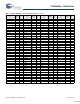
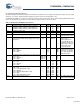
Table 12. DC GPIO Specifications
Symbol Description Min Typ Max Units Notes
R
PU
Pull up Resistor 4 5.6 8 kΩ
R
PD
Pull down Resistor 4 5.6 8 kΩ
V
OH
High Output Level 3.5 – – V IOH = 10 mA, Vdd = 4.75 to 5.25V (8 total
loads, 4 on even port pins (for example,
P0[2], P1[4]), 4 on odd port pins (for
example, P0[3], P1[5])).
V
OL
Low Output Level – – 0.75 V IOL = 25 mA, Vdd = 4.75 to 5.25V (8 total
loads, 4 on even port pins (for example,
P0[2], P1[4]), 4 on odd port pins (for
example, P0[3], P1[5])). Total IOL budget
of 150 mA.
V
IL
Input Low Level – – 0.8 V Vdd = 4.75 to 5.25
V
IH
Input High Level 2.2 – V Vdd = 4.75 to 5.25
V
H
Input Hysterisis – 60 – mV
I
IL
Input Leakage (Absolute Value) – 1 – nA Gross tested to 1 μA
C
IN
Capacitive Load on Pins as Input – 3.5 10 pF Package and pin dependent.
Temp = 25
o
C
C
OUT
Capacitive Load on Pins as Output – 3.5 10 pF Package and pin dependent.
Temp = 25
o
C
[+] Feedback