
Nonvolatile Programmable System-on-Chip Specification Sheet

PRELIMINARY CY8CNP102B, CY8CNP102E
Document #: 001-43991 Rev. *D Page 15 of 38
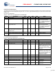
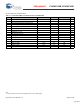
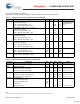
DC POR, SMP, and LVD Specifications
Table 12. 3.3V DC POR, SMP, and LVD Specifications (CY8CNP102B)
Symbol Description Min Typ Max Units
Vdd Value for PPOR Trip (positive ramp)
V
PPOR0R
PORLEV[1:0] = 00b 2.91 V
Vdd Value for PPOR Trip (negative ramp)
V
PPOR0
PORLEV[1:0] = 00b 2.82 V
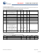
PPOR Hysteresis
V
PH0
PORLEV[1:0] = 00b 92 mV
V
PH1
PORLEV[1:0] = 01b 0 mV
V
PH2
PORLEV[1:0] = 10b 0 mV
Vdd Value for LVD Trip
V
LVD0
VM[2:0] = 000b 2.86 2.92 2.98
[2]
V
V
LVD1
VM[2:0] = 001b 2.96 3.02 3.08 V
V
LVD2
VM[2:0] = 010b 3.07 3.13 3.20 V
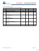
Vdd Value for SMP Trip
V
PUMP0
VM[2:0] = 000b 2.96 3.02 3.08 V
V
PUMP1
VM[2:0] = 001b 3.03 3.10 3.16 V
V
PUMP2
VM[2:0] = 010b 3.18 3.25 3.32 V
Note
2. Always greater than 50 mV above PPOR (PORLEV = 00) for falling supply.
[+] Feedback