
Nonvolatile Programmable System-on-Chip Specification Sheet

PRELIMINARY CY8CNP102B, CY8CNP102E
Document #: 001-43991 Rev. *D Page 20 of 38
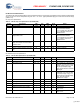
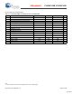
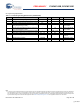
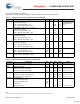
AC Analog Output Buffer Specifications
CRCPRS
(PRS Mode)
Maximum Input Clock Frequency – – 24.6 MHz 3.0V ≤ Vcc ≤ 3.6V
CRCPRS
(CRC Mode)
Maximum Input Clock Frequency – – 24.6 MHz 3.0V ≤ Vcc ≤ 3.6V.
SPIM Maximum Input Clock Frequency – – 8.2 MHz Maximum data rate at
4.1 MHz due to 2 x
over clocking.
SPIS Maximum Input Clock Frequency – – 4.1 ns
Width of SS_ Negated Between Transmissions 50
[8]
– – ns
Transmitter Maximum Input Clock Frequency
Vcc ≥ 3.0V, 2 Stop Bits
– – 24.6 MHz Maximum data rate at
3.08 MHz due to 8 x
over clocking.
– – 49.2 MHz Maximum data rate at
6.15 MHz due to 8 x
over clocking.
Receiver Maximum Input Clock Frequency – – 24.6 MHz Maximum data rate at
3.08 MHz due to 8 x
over clocking.
Vcc ≥ 3.0V, 2 Stop Bits – – 49.2 MHz Maximum data rate at
6.15 MHz due to 8 x
over clocking.
Table 18. 3.3V AC Digital Block Specifications (CY8CNP102B) (continued)
Function Description Min Typ Max Units Notes
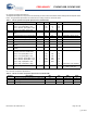
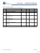
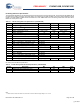
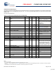
Table 19. 3.3V AC Analog Output Buffer Specifications (CY8CNP102B)
Symbol Description Min Typ Max Units
T
ROB
Rising Settling Time to 0.1%, 1V Step, 100pF Load
Power = Low – – 4.7 μs
Power = High – – 4.7 μs
T
SOB
Falling Settling Time to 0.1%, 1V Step, 100pF Load
Power = Low – – 4 μs
Power = High – – 4 μs
SR
ROB
Rising Slew Rate (20% to 80%), 1V Step, 100pF Load
Power = Low 0.36 – – V/μs
Power = High 0.36 – – V/μs
SR
FOB
Falling Slew Rate (80% to 20%), 1V Step, 100pF Load
Power = Low 0.4 – – V/μs
Power = High 0.4 – – V/μs
BW
OB
Small Signal Bandwidth, 20mV
pp
, 3dB BW, 100pF Load
Power = Low 0.7 – – MHz
Power = High 0.7 – – MHz
BW
OB
Large Signal Bandwidth, 1V
pp
, 3dB BW, 100pF Load
Power = Low 200 – – kHz
Power = High 200 – – kHz
[+] Feedback