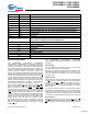
CYDC256B16, CYDC128B16, CYDC064B16, CYDC128B08, CYDC064B08 1.8V 4k/8k/16k x 16 and 8k/16k x 8 ConsuMoBL Dual-Port Static RAM Features • Lead (Pb)-free 14 x 14 x 1.
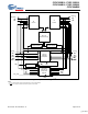
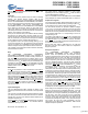
CYDC256B16, CYDC128B16, CYDC064B16, CYDC128B08, CYDC064B08 I/O[15:0]R I/O[15:0]L UBR UBL LBL LBR IO Control IO Control 16K X 16 Dual Ported Array Address Decode Address Decode A[13:0]L CE L A [13:0]R CE R Interrupt Arbitration Semaphore OE L R/W L SEML BUSY L INTL IRR0 ,IRR1 Mailboxes INTR OE R R/W R SEMR BUSY R M/S Input Read Register and Output Drive Register CEL OEL R/WL CE R OE R R/W R ODR0 - ODR4 SFEN Figure 1. Top Level Block Diagram[1, 2] Notes: 1.
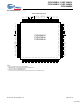
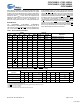
CYDC256B16, CYDC128B16, CYDC064B16, CYDC128B08, CYDC064B08 Pin Configurations [3, 4, 5, 6, 7] A3R A2R A1R A0R UBR LBR OER R/WR VSS ODR4 ODR3 ODR2 VSS ODR1 ODR0 VSS SFEN R/WL OEL LBL UBL A0L A1L A2L A3L 100-Pin TQFP (Top View) 100 99 98 97 96 95 94 93 92 91 90 89 88 87 86 85 84 83 82 81 80 79 78 77 76 A4L 1 75 A4R A5L 2 74 A5R A6L 3 73 A6R A7L 4 72 A7R A8L 5 71 A8R CEL 6 70 CER SEML 7 69 SEMR INTL 8 68 INTR BUSYL 9 67 BUSYR 66 A9R 65 A10R 64
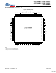
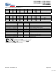
CYDC256B16, CYDC128B16, CYDC064B16, CYDC128B08, CYDC064B08 Pin Configurations (continued)[7, 8, 9, 10] A3R A2R A1R A0R UBR LBR OER R/WR VSS ODR4 ODR3 ODR2 VSS ODR1 ODR0 VSS SFEN R/WL OEL LBL UBL A0L A1L A2L A3L 100-pin TQFP (Top View) 100 99 98 97 96 95 94 93 92 91 90 89 88 87 86 85 84 83 82 81 80 79 78 77 76 A4L 1 75 A4R A5L 2 74 A5R A6L 3 73 A6R A7L 4 72 A7R A8L 5 71 A8R CEL 6 70 CER SEML 7 69 SEMR INTL 8 68 INTR BUSYL 9 67 BUSYR A9L 10 66
CYDC256B16, CYDC128B16, CYDC064B16, CYDC128B08, CYDC064B08 Pin Definitions Left Port Right Port Description CEL CER Chip Enable R/WL R/WR Read/Write Enable OEL OER Output Enable A0L–A13L A0R–A13R Address (A0–A11 for 4k devices; A0–A12 for 8k devices; A0–A13 for 16k devices). I/O0L–I/O15L I/O0R–I/O15R Data Bus Input/Output for x16 devices; I/O0–I/O7 for x8 devices. SEML SEMR Semaphore Enable UBL UBR Upper Byte Select (I/O8–I/O15 for x16 devices; Not applicable for x8 devices).
CYDC256B16, CYDC128B16, CYDC064B16, CYDC128B08, CYDC064B08 then the SEM pin must be asserted instead of the CE pin, and OE must also be asserted. Interrupts The upper two memory locations may be used for message passing.
CYDC256B16, CYDC128B16, CYDC064B16, CYDC128B08, CYDC064B08 When reading a semaphore, all sixteen/eight data lines output the semaphore value. The read value is latched in an output register to prevent the semaphore from changing state during a write from the other port. If both ports attempt to access the semaphore within tSPS of each other, the semaphore will definitely be obtained by one side or the other, but there is no guarantee which side will control the semaphore.
CYDC256B16, CYDC128B16, CYDC064B16, CYDC128B08, CYDC064B08 Table 3. Input Read Register Operation[16, 19] SFEN H L CE L L R/W OE H UB L H LB L L ADDR I/O0–I/O1 I/O2–I/O15 [17] L x0000-Max VALID X L x0000 UB LB ADDR [18] VALID [17] VALID X Mode Standard Memory Access IRR Read Table 4.
CYDC256B16, CYDC128B16, CYDC064B16, CYDC128B08, CYDC064B08 Maximum Ratings[23] Output Current into Outputs (LOW)............................. 90 mA (Above which the useful life may be impaired. For user guidelines, not tested.) Storage Temperature ................................. –65°C to +150°C Ambient Temperature with Power Applied............................................. –55°C to +125°C Supply Voltage to Ground Potential ............... –0.5V to +3.3V DC Voltage Applied to Outputs in High-Z State.
CYDC256B16, CYDC128B16, CYDC064B16, CYDC128B08, CYDC064B08 Electrical Characteristics for VCC = 1.8V (continued) Over the Operating Range Parameter IIX P1 I/O P2 I/O Voltage Voltage Description Input Leakage Current CYDC256B16, CYDC128B16, CYDC064B16, CYDC128B08, CYDC064B08 CYDC256B16, CYDC128B16, CYDC064B16, CYDC128B08, CYDC064B08 -40 -55 Min. Typ. Max. Min. Typ. Max. Unit 1.8V 1.8V –1 1 –1 1 µA 2.5V 2.5V –1 1 –1 1 µA 3.0V 3.
CYDC256B16, CYDC128B16, CYDC064B16, CYDC128B08, CYDC064B08 Electrical Characteristics for VCC = 2.5V Over the Operating Range Parameter Description CYDC256B16, CYDC128B16, CYDC064B16, CYDC128B08, CYDC064B08 CYDC256B16, CYDC128B16, CYDC064B16, CYDC128B08, CYDC064B08 -40 -55 P1 I/O P2 I/O Voltage Voltage Min. 2.5V (any port) 2.0 2.1 Typ. Max. Min. Typ. Max. Unit VOH Output HIGH Voltage (IOH = –2 mA) 2.0 V Output HIGH Voltage (IOH = –2 mA) 3.
CYDC256B16, CYDC128B16, CYDC064B16, CYDC128B08, CYDC064B08 Electrical Characteristics for 3.0V Over the Operating Range Parameter Description CYDC256B16, CYDC128B16, CYDC064B16, CYDC128B08, CYDC064B08 CYDC256B16, CYDC128B16, CYDC064B16, CYDC128B08, CYDC064B08 -40 -55 P1 I/O P2 I/O Voltage Voltage Min. 3.0V (any port) 2.1 Typ. Max. Min. Typ. Max. Unit VOH Output HIGH Voltage (IOH = –2 mA) 2.1 V VOL Output LOW Voltage (IOL = 2 mA) 3.0V (any port) 0.4 0.
CYDC256B16, CYDC128B16, CYDC064B16, CYDC128B08, CYDC064B08 AC Test Loads and Waveforms 7 3.0V/2.5V/1.8V 3.0V/2.5V/1.8V R1 RTH = 6 kΩ OUTPUT OUTPUT R1 OUTPUT C = 30 pF C = 30 pF R2 VTH = 0.8V (a) Normal Load (Load 1) (b) Thévenin Equivalent (Load 1) 1.8V R1 1022Ω 13500Ω 1.8V R2 792Ω 10800Ω GND 10% R2 (c) Three-State Delay (Load 2) (Used for tLZ, tHZ, tHZWE, and tLZWE including scope and jig) ALL INPUT PULSES 3.0V/2.
CYDC256B16, CYDC128B16, CYDC064B16, CYDC128B08, CYDC064B08 Switching Characteristics for VCC = 1.8V Over the Operating Range[27] (continued) Parameter Description CYDC256B16, CYDC128B16, CYDC064B16, CYDC128B08, CYDC064B08 CYDC256B16, CYDC128B16, CYDC064B16, CYDC128B08, CYDC064B08 -40 -55 Min. Max. Min. Max.
CYDC256B16, CYDC128B16, CYDC064B16, CYDC128B08, CYDC064B08 Switching Characteristics for VCC = 2.5V Over the Operating Range Parameter Description CYDC256B16, CYDC128B16, CYDC064B16, CYDC128B08, CYDC064B08 CYDC256B16, CYDC128B16, CYDC064B16, CYDC128B08, CYDC064B08 -40 -55 Min. Max. Min. Max.
CYDC256B16, CYDC128B16, CYDC064B16, CYDC128B08, CYDC064B08 Switching Characteristics for VCC = 2.5V Over the Operating Range (continued) Parameter Description CYDC256B16, CYDC128B16, CYDC064B16, CYDC128B08, CYDC064B08 CYDC256B16, CYDC128B16, CYDC064B16, CYDC128B08, CYDC064B08 -40 -55 Min. Max. Min. Max.
CYDC256B16, CYDC128B16, CYDC064B16, CYDC128B08, CYDC064B08 Switching Characteristics for VCC = 3.0V Over the Operating Range (continued) Parameter Description tHZWE[30, 31] R/W LOW to High Z [30, 31] R/W HIGH to Low Z tLZWE tWDD[32] tDDD[32] CYDC256B16, CYDC128B16, CYDC064B16, CYDC128B08, CYDC064B08 CYDC256B16, CYDC128B16, CYDC064B16, CYDC128B08, CYDC064B08 -40 -55 Min. Max. Min. 15 0 Unit Max.
CYDC256B16, CYDC128B16, CYDC064B16, CYDC128B08, CYDC064B08 Switching Waveforms Read Cycle No.1 (Either Port Address Access)[36, 37, 38] tRC ADDRESS tOHA DATA OUT tAA tOHA PREVIOUS DATA VALID DATA VALID Read Cycle No.2 (Either Port CE/OE Access)[36, 39, 40] tACE CE and LB or UB tHZCE tDOE OE tHZOE tLZOE DATA VALID DATA OUT tLZCE tPU CURRENT tPD ICC ISB Read Cycle No. 3 (Either Port)[36, 38, 41, 42] tRC ADDRESS tOHA tAA UB or LB tHZCE tLZCE tABE CE tHZCE tACE tLZCE DATA OUT Notes: 36.
CYDC256B16, CYDC128B16, CYDC064B16, CYDC128B08, CYDC064B08 Switching Waveforms (continued) Write Cycle No.1: R/W Controlled Timing[41, 42, 43, 44, 45, 46] tWC ADDRESS tHZOE [47] OE tAW CE [45, 46] tPWE[44] tSA tHA R/W tHZWE[47] DATA OUT tLZWE NOTE 48 NOTE 48 tSD tHD DATA IN Write Cycle No. 2: CE Controlled Timing[41, 42, 43, 48] tWC ADDRESS tAW CE [45, 46] tSA tSCE tHA R/W tSD tHD DATA IN Notes: 43.
CYDC256B16, CYDC128B16, CYDC064B16, CYDC128B08, CYDC064B08 Switching Waveforms (continued) Semaphore Read After Write Timing, Either Side[49, 50] tSAA A0–A2 VALID ADRESS VALID ADRESS tAW tACE tHA SEM tOHA tSCE tSOP tSD I/O0 DATAIN VALID tSA tPWE DATAOUT VALID tHD R/W tSWRD tDOE tSOP OE WRITE CYCLE READ CYCLE Timing Diagram of Semaphore Contention[51, 52] A0L–A2L MATCH R/WL SEML tSPS A0R–A2R MATCH R/WR SEMR Notes: 49.
CYDC256B16, CYDC128B16, CYDC064B16, CYDC128B08, CYDC064B08 Switching Waveforms (continued) Timing Diagram of Read with BUSY (M/S=HIGH)[53] tWC ADDRESSR MATCH tPWE R/WR tHD tSD DATA INR VALID tPS ADDRESSL MATCH tBLA tBHA BUSYL tBDD tDDD DATAOUTL VALID tWDD Write Timing with Busy Input (M/S = LOW) tPWE R/W BUSY tWB tWH Note: 53. CEL = CER = LOW. Document #: 001-01638 Rev.
CYDC256B16, CYDC128B16, CYDC064B16, CYDC128B08, CYDC064B08 Switching Waveforms (continued) Busy Timing Diagram No.1 (CE Arbitration) CEL Valid First[54] ADDRESSL,R ADDRESS MATCH CEL tPS CER tBLC tBHC BUSYR CER Valid First ADDRESS L,R ADDRESS MATCH CER tPS CEL tBLC tBHC BUSYL Busy Timing Diagram No.
CYDC256B16, CYDC128B16, CYDC064B16, CYDC128B08, CYDC064B08 Switching Waveforms (continued) Interrupt Timing Diagrams Left Side Sets INTR: ADDRESSL tWC WRITE 1FFF (OR 1/3FFF) tHA[55] CEL R/WL INTR tINS [56] Right Side Clears INTR: tRC READ 1FFF (OR 1/3FFF) ADDRESSR CER tINR [56] R/WR OER INTR Right Side Sets INTL: ADDRESSR tWC WRITE 1FFE (OR 1/3FFE) tHA[55] CER R/WR INTL [56] tINS Left Side Clears INTL: tRC READ 1FFE OR 1/3FFE) ADDRESSR CEL tINR[56] R/WL OEL INTL Notes: 55.
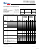
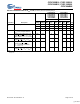
CYDC256B16, CYDC128B16, CYDC064B16, CYDC128B08, CYDC064B08 Ordering Information 16k x16 1.8V Asynchronous Dual-Port SRAM Speed (ns) Ordering Code Package Name Package Type Operating Range 40 CYDC256B16-40AXC AZ0AB 100-pin Lead-free TQFP Commercial 55 CYDC256B16-55AXC AZ0AB 100-pin Lead-free TQFP Commercial 55 CYDC256B16-55AXI AZ0AB 100-pin Lead-free TQFP Industrial 8k x16 1.
CYDC256B16, CYDC128B16, CYDC064B16, CYDC128B08, CYDC064B08 Package Diagram 100-Pin Thin Plastic Quad Flat Pack (TQFP) A100 51-85048-*C All products and company names mentioned in this document may be the trademarks of their respective holders. Document #: 001-01638 Rev. *E Page 25 of 26 © Cypress Semiconductor Corporation, 2006. The information contained herein is subject to change without notice.
CYDC256B16, CYDC128B16, CYDC064B16, CYDC128B08, CYDC064B08 Document History Page Document Title: CYDC256B16/CYDC128B16/CYDC064B16/CYDC128B08/CYDC064B08 1.8V 4k/8k/16k x 16 and 8k/16k x 8 ConsuMoBL Dual-Port Static RAM Document Number: 001-01638 REV. ECN NO. Issue Date Orig. of Change Description of Change ** 385185 SEE ECN YDT New data sheet *A 396697 SEE ECN KGH Updated ISB2 and ISB4 typo to mA. Updated tINS and tINR for -55 to 31ns.