
Transceiver with Reclocker Specification Sheet


CYV15G0404DXB
Document #: 38-02097 Rev. *B Page 12 of 44
CYV15G0404DXB HOTLink II Operation
The CYV15G0404DXB is a highly configurable, independent
clocking, quad-channel transceiver designed to support reliable
transfer of large quantities of data, using high speed serial links
from multiple sources to multiple destinations. This device
supports four single byte channels.
CYV15G0404DXB Transmit Data Path
Input Register
The bits in the Input Register for each channel support different
assignments, based on if the input data is encoded or
unencoded. These assignments are shown in Table 1.
When the ENCODER is enabled, each input register captures
eight data bits and two control bits on each input clock cycle.
When the encoder is bypassed, the control bits are part of the
preencoded 10-bit character.
When the encoder is enabled, the TXCTx[1:0] bits are inter-
preted along with the associated TXDx[7:0] character to
generate a specific 10-bit transmission character.
Phase Align Buffer
Data from each input register is passed to the associated phase
align buffer, when the TXDx[7:0] and TXCTx[1:0] input registers
are clocked using TXCLKx¦ (TXCKSELx = 0 and TXRATEx = 0).
When the TXDx[7:0] and TXCTx[1:0] input registers are clocked
using REFCLKx± (TXCKSELx = 1) and REFCLKx± is a full rate
clock, the associated phase alignment buffer in the transmit path
is bypassed. These buffers are used to absorb clock phase
differences between the TXCLKx input clock and the internal
character clock for that channel.
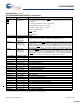
Factory Test Modes
SCANEN2 LVTTL input,
internal pull down
Factory Test 2. SCANEN2 input is for factory testing only. Leave this input as a NO
CONNECT or GND only.
TMEN3 LVTTL input,
internal pull down
Factory Test 3. TMEN3 input is for factory testing only. Leave this input as a NO
CONNECT or GND only.
Analog I/O
OUTA1±
OUTB1±
OUTC1±
OUTD1±
CML Differential
Output
Primary Differential Serial Data Output. The OUTx1± PECL-compatible CML
outputs (+3.3V referenced) are capable of driving terminated transmission lines or
standard fiber-optic transmitter modules, and must be AC coupled for PECL
compatible connections.
OUTA2±
OUTB2±
OUTC2±
OUTD2±
CML Differential
Output
Secondary Differential Serial Data Output. The OUTx2± PECL-compatible CML outputs
(+3.3V referenced) are capable of driving terminated transmission lines or standard fiber
optic transmitter modules, and must be AC coupled for PECL compatible connections.
INA1±
INB1±
INC1±
IND1±
Differential Input Primary Differential Serial Data Input. The INx1± input accepts the serial data
stream for deserialization and decoding. The INx1± serial stream is passed to the
receive CDR circuit to extract the data content when INSELx = HIGH.
INA2±
INB2±
INC2±
IND2±
Differential Input Secondary Differential Serial Data Input. The INx2± input accepts the serial data
stream for deserialization and decoding. The INx2± serial stream is passed to the
receiver CDR circuit to extract the data content when INSELx = LOW.
JTAG Interface
TMS LVTTL Input,
internal pull up
Test Mode Select. Used to control access to the JTAG Test Modes. If maintained
high for ≥5 TCLK cycles, the JTAG test controller is reset.
TCLK LVTTL Input,
internal pull down
JTAG Test Clock.
TDO 3-State LVTTL Output Test Data Out. JTAG data output buffer. High-Z while JTAG test mode is not selected.
TDI LVTTL Input,
internal pull up
Test Data In. JTAG data input port.
TRST
LVTTL Input,
internal pull up
JTAG reset signal. When asserted (LOW), this input asynchronously resets the
JTAG test access port controller.
Power
V
CC
+3.3V Power.
GND Signal and Power Ground for all internal circuits.
Pin Definitions (continued)
CYV15G0404DXB Quad HOTLink II Transceiver
Name I/O Characteristics Signal Description
[+] Feedback [+] Feedback