
Transceiver with Reclocker Specification Sheet


CYV15G0404DXB
Document #: 38-02097 Rev. *B Page 19 of 44
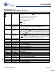
When the 10B/8B decoder is bypassed, the framed 10-bit value
is presented to the associated output register, along with a status
output signal indicating if the character in the output register is
one of the selected framing characters. The bit usage and
mapping of the external signals to the raw 10B transmission
character is shown in Table 8.
The COMDETx status output operates the same regardless of
the bit combination selected for character framing by the
FRAMCHARx latch. COMDETx is HIGH when the character in
the output register contains the selected framing character at the
proper character boundary, and LOW for all other bit combina-
tions.
When the low-latency framer and half rate receive port clocking
are also enabled, the framer stretches the recovered clock to the
nearest 20-bit boundary such that the rising edge of RXCLKx+
occurs when COMDETx is present on the associated output bus.
When the Cypress or alternate mode framer is enabled and half
rate receive port clocking is also enabled, the output clock is not
modified when framing is detected, but a single pipeline stage
may be added or subtracted from the data stream by the framer
logic such that the rising edge of RXCLKx+ occurs when
COMDETx is present on the associated output bus.
This adjustment only occurs when the framer is enabled. When
the framer is disabled, the clock boundaries are not adjusted,
and COMDETx may be asserted during the rising edge of
RXCLKx– (if an odd number of characters were received
following the initial framing).
Receive Status Bits
When the 10B/8B decoder is enabled, each character presented
at the output register includes three associated status bits.
These bits are used to identify
■ If the contents of the data bus are valid
■ The type of character present
■ The state of receive BIST operations
■ Character violations
These conditions often overlap; for example, a valid data
character received with incorrect running disparity is not reported
as a valid data character. It is instead reported as a decoder
violation of some specific type. This implies a hierarchy or priority
level to the various status bit combinations. The hierarchy and
value of each status are listed in Table 11.
A second status mapping, listed in Table 11, is used when the
receive channel is configured for BIST operation. This status is
used to report receive BIST status and progress.
BIST Status State Machine
When a receive path is enabled to look for and compare the
received data stream with the BIST pattern, the RXSTx[2:0] bits
identify the present state of the BIST compare operation.
The BIST state machine has multiple states, as shown in
Figure 2 and Table 11. When the receive PLL detects an
out-of-lock condition, the BIST state is forced to the Start-of-BIST
state, regardless of the present state of the BIST state machine.
If the number of detected errors ever exceeds the number of
valid matches by greater than 16, the state machine is forced to
the WAIT_FOR_BIST state where it monitors the receive path for
the first character of the next BIST sequence (D0.0). Also, if the
Elasticity Buffer ever hits an overflow/underflow condition, the
status is forced to the BIST_START until the buffer is re-centered
(approximately nine character periods).
To ensure compatibility between the source and destination
systems when operating in BIST modes, the sending and
receiving ends of the link must use the same receive clock
configuration.
Device Configuration and Control Interface
The CYP(V)15G0404DX is highly configurable through the
configuration interface. The configuration interface allows the
device to be configured globally or allows each channel to be
configured independently. Table 9 lists the configuration latches
within the device including the initialization value of the latches
upon the assertion of RESET
. Table 10 shows how the latches
are mapped in the device. Each row in the Table 10 maps to a
8-bit latch bank. There are 16 such write-only latch banks. When
WREN
= 0, the logic value in the DATA[7:0] is latched to the latch
bank specified by the values in ADDR[3:0]. The second column
of Tabl e 10 specifies the channels associated with the corre-
sponding latch bank. For example, the first three latch banks (0,1
and 2) consist of configuration bits for channel A. The latch banks
Table 7. Output Register Bit Assignments
Signal Name
BYPASS ACTIVE
(DECBYPx = 0)
DECODER
(DECBYP = 1)
RXSTx[2] (LSB) COMDETx RXSTx[2]
RXSTx[1] DOUTx[0] RXSTx[1]
RXSTx[0] DOUTx[1] RXSTx[0]
RXDx[0] DOUTx[2] RXDx[0]
RXDx[1] DOUTx[3] RXDx[1]
RXDx[2] DOUTx[4] RXDx[2]
RXDx[3] DOUTx[5] RXDx[3]
RXDx[4] DOUTx[6] RXDx[4]
RXDx[5] DOUTx[7] RXDx[5]
RXDx[6] DOUTx[8] RXDx[6]
RXDx[7] (MSB) DOUTx[9] RXDx[7]
Table 8. Decoder Bypass Mode
Signal Name Bus Weight 10 Bit Name
RXSTx[2] (LSB) COMDETx
RXSTx[1] 2
0
a
RXSTx[0] 2
1
b
RXDx[0] 2
2
c
RXDx[1] 2
3
d
RXDx[2] 2
4
e
RXDx[3] 2
5
i
RXDx[4] 2
6
f
RXDx[5] 2
7
g
RXDx[6] 2
8
h
RXDx[7] (MSB) 2
9
j
[+] Feedback [+] Feedback