
Transceiver with Reclocker Specification Sheet

CYV15G0404DXB
Document #: 38-02097 Rev. *B Page 2 of 44
The CYV15G0404DXB satisfies the SMPTE-259M and
SMPTE-292M compliance according to SMPTE EG34-1999
Pathological Test Requirements.
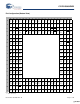
As a second generation HOTLink device, the CYV15G0404DXB
extends the HOTLink family with enhanced levels of integration and
faster data rates, while maintaining serial link compatibility (data,
command, and BIST) with other HOTLink devices. The transmit
(TX) section of the CYV15G0404DXB Quad HOTLink II consists of
four independent byte-wide channels. Each channel accepts
either 8-bit data characters or preencoded 10-bit transmission
characters. Data characters may be passed from the transmit
input register to an integrated 8B/10B Encoder to improve their
serial transmission characteristics. These encoded characters
are then serialized and output from dual Positive ECL (PECL)
compatible differential transmission-line drivers at a bit rate of
either 10 or 20 times the input reference clock for that channel.
The receive (RX) section of the CYV15G0404DXB Quad
HOTLink II consists of four independent byte wide channels.
Each channel accepts a serial bit stream from one of two
PECL-compatible differential line receivers, and using a
completely integrated Clock and Data Recovery PLL, recovers
the timing information necessary for data reconstruction. Each
recovered bit stream is deserialized and framed into characters,
8B/10B decoded, and checked for transmission errors.
Recovered decoded characters are then written to an internal
elasticity buffer, and presented to the destination host system.
The integrated 8B/10B encoder or decoder may be bypassed for
systems that present externally encoded or scrambled data at
the parallel interface.
The parallel IO interface may be configured for numerous forms
of clocking to provide the highest flexibility in system archi-
tecture. In addition to clocking the transmit path with a local
reference clock, the receive interface may also be configured to
present data relative to a recovered clock or to a local reference
clock.
Each transmit and receive channel contains an independent
BIST pattern generator and checker. This BIST hardware allows
at speed testing of the high speed serial data paths in each
transmit and receive section, and across the interconnecting
links.
The CYV15G0404DXB is ideal for port applications where
different data rates and serial interface standards are necessary
for each channel. Some applications include multi-format routers
and switchers.
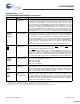
CYV15G0404DXB Transceiver Logic Block Diagram
x10
Serializer
Phase
Encoder
8B/10B
Decoder
8B/10B
x11
Framer
Deserializer
TX
RX
x10
Serializer
Encoder
8B/10B
Decoder
8B/10B
x11
Framer
Deserializer
TX
RX
x10
Serializer
Encoder
8B/10B
Decoder
8B/10B
x11
Framer
Deserializer
TX
RX
x10
Serializer
Encoder
8B/10B
Decoder
8B/10B
x11
Framer
Deserializer
TX
RX
TXDA[7:0]
RXDA[7:0]
TXDB[7:0]
RXDB[7:0]
TXDC[7:0]
RXDC[7:0]
TXDD[7:0]
RXDD[7:0]
OUTA1±
OUTA2±
INA1±
INA2±
OUTB1±
OUTB2±
INB1±
INB2±
OUTC1±
OUTC2±
INC1±
INC2±
OUTD1±
OUTD2±
IND1±
IND2±
Align
Buffer
Phase
Align
Buffer
Phase
Align
Buffer
Phase
Align
Buffer
Elasticity
Buffer
Elasticity
Buffer
Elasticity
Buffer
Elasticity
Buffer
TXCTA[1:0]
RXSTA[2:0]
TXCTB[1:0]
RXSTB[2:0]
TXCTC[1:0]
RXSTC[2:0]
TXCTD[1:0]
RXSTD[2:0]
REFCLKA±
REFCLKB±
REFCLKC±
REFCLKD±
[+] Feedback [+] Feedback