
Transceiver with Reclocker Specification Sheet


CYV15G0404DXB
Document #: 38-02097 Rev. *B Page 20 of 44
12, 13, and 14 consist of global configuration bits and the last
latch bank (15) is the mask latch bank that can be configured to
perform bit-by-bit configuration.
Global Enable Function
The global enable function, controlled by the GLENx bits, is a
feature that is used to reduce the number of write operations
needed to setup the latch banks. This function is beneficial in
systems that use a common configuration in multiple channels.
The GLENx bit is present in bit 0 of latch banks 0 through 11 only.
Its default value (1) enables the global update of the latch bank's
contents. Setting the GLENx bit to 0 disables this functionality.
Latch Banks 12, 13, and 14 load values in the related latch banks
in a global manner. A write operation to latch bank 12 could do
a global write to latch banks 0, 3, 6, and 9 depending on the value
of GLENx in these latch banks; latch bank 13 could do a global
write to latch banks 1, 4, 7, and 10; and latch banks 14 could do
a global write to latch banks 2, 5, 8, and 11. The GLENx bit
cannot be modified by a global write operation.
Force Global Enable Function
FGLENx forces the global update of the target latch banks, but
does not change the contents of the GLENx bits. If FGLENx = 1
for the associated global channel, FGLENx forces the global
update of the target latch banks.
Mask Function
An additional latch bank (15) is used as a global mask vector to
control the update of the configuration latch banks on a bit-by-bit
basis. A logic 1 in a bit location allows for the update of that same
location of the target latch bank(s), whereas a logic 0 disables it.
The reset value of this latch bank is FFh, thereby making its use
optional by default. The mask latch bank is not maskable. The
FGLEN functionality is not affected by the bit 0 value of the mask
latch bank.
Latch Types
There are two types of latch banks: static (S) and dynamic (D).
Each channel is configured by two static and one dynamic latch
bank. The S type contain those settings that normally do not
change for a given application, while the D type controls the
settings that could change dynamically during the application's
lifetime.The first row of latches for each channel (address
numbers 0, 3, 7, and 10) are the static receiver control latches.
The second row of latches for each channel (address numbers
1, 4, 8, and 11) are the static transmitter control latches. The third
row of latches for each channel (address numbers 2, 5, 9, and
12) are the dynamic control latches that are associated with
enabling dynamic functions within the device.
Latch Bank 14 is also useful for those users that do not need the
latch-based programmable feature of the device. This latch bank
could be used in those applications that do not need to modify
the default value of the static latch banks, and that can afford a
global (that is, not independent) control of the dynamic signals.
In this case, this feature becomes available when ADDR[3:0] is
left unchanged with a value of “1110” and WREN
is left asserted.
The signals present in DATA[7:0] effectively become global
control pins, and for the latch banks 2, 5, 8, and 11.
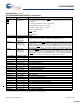
Table 9. Device Configuration and Control Latch Descriptions
Name Signal Description
RFMODEA[1:0]
RFMODEB[1:0]
RFMODEC[1:0]
RFMODED[1:0]
Reframe Mode Select. The initialization value of the RFMODEx [1:0] latches = 10. RFMODEx is used to select
the operating mode of the framer. When RFMODEx[1:0] = 00, the low-latency framer is selected. This frames
on each occurrence of the selected framing character(s) in the received data stream. This mode of framing
stretches the recovered clock for one or multiple cycles to align that clock with the recovered data. When
RFMODEx[1:0] = 01, the alternate mode Multi-Byte parallel framer is selected. This requires detection of the
selected framing character(s) in the received serial bit stream, on identical 10-bit boundaries, on four directly
adjacent characters. The recovered character clock remains in the same phasing regardless of character
offset. When RFMODEx[1:0] =10, the Cypress-mode Multi-Byte parallel framer is selected. This requires a
pair of the selected framing character(s), on identical 10-bit boundaries, within a span of 50 bits, before the
character boundaries are adjusted. The recovered character clock remains in the same phasing regardless of
character offset. RFMODEx[1:0] = 11 is reserved for test.
FRAMCHARA
FRAMCHARB
FRAMCHARC
FRAMCHARD
Framing Character Select. The initialization value of the FRAMCHARx latch = 1. FRAMCHARx is used to
select the character or portion of a character used for framing of each channel’s received data stream. When
FRAMCHARx = 1, the framer looks for either disparity of the K28.5 character. When FRAMCHARx = 0, the
framer looks for either disparity of the 8-bit Comma characters. The specific bit combinations of these framing
characters are listed in Table 6.
DECMODEA
DECMODEB
DECMODEC
DECMODED
Receiver Decoder Mode Select. The initialization value of the DECMODEx latch = 1. DECMODEx selects
the Decoder Mode used for the associated channel. When DECMODEx = 1 and decoder is enabled, the
Cypress Decoding Mode is used. When DECMODEx = 0 and decoder is enabled, the Alternate Decoding
mode is used. When the decoder is enabled (DECBYPx = 1), the 10-bit transmission characters are decoded
using Table 14 and Table 15. The column used in the Special Characters Table 15 is determined by the
DECMODEx latch.
DECBYPA
DECBYPB
DECBYPC
DECBYPD
Receiver Decoder Bypass. The initialization value of the DECBYPx latch = 1. DECBYPx selects if the
Receiver Decoder is enabled or bypassed. When DECBYPx = 1, the decoder is enabled and the Decoder
Mode is selected by DECMODEx. When DECBYPx = 0, the decoder is bypassed and raw 10-bit characters
are passed through the receiver.
[+] Feedback [+] Feedback