
Transceiver with Reclocker Specification Sheet


CYV15G0404DXB
Document #: 38-02097 Rev. *B Page 21 of 44
RXCKSELA
RXCKSELB
RXCKSELC
RXCKSELD
Receive Clock Select. The initialization value of the RXCKSELx latch = 1. RXCKSELx selects the receive
clock source used to transfer data to the Output Registers and the clock source for the RXCLK± output. When
RXCKSELx = 1, the associated Output Registers, are clocked by REFCLKx± at the associated RXCLKx±
output buffer. When RXCKSELx = 0, the associated Output Registers, are clocked by the Recovered Byte
clock at the associated RXCLKx± output buffer. These output clocks may operate at the character-rate or half
the character-rate as selected by RXRATEx.
RXRATEA
RXRATEB
RXRATEC
RXRATED
Receive Clock Rate Select. The initialization value of the RXRATEx latch = 1. RXRATEx is used to select the
rate of the RXCLKx± clock output.
When RXRATEx = 1 and RXCKSELx = 0, the RXCLKx± clock outputs are complementary clocks that follow
the recovered clock operating at half the character rate. Data for the associated receive channels should be
latched alternately on the rising edge of RXCLKx+ and RXCLKx–.
When RXRATEx = 0 and RXCKSELx = 0, the RXCLKx± clock outputs are complementary clocks that follow
the recovered clock operating at the character rate. Data for the associated receive channels should be latched
on the rising edge of RXCLKx+ or falling edge of RXCLKx–.
When RXRATEx = 1 with RXCKSELx = 1 and REFCLKx± is a full rate clock, the RXCLKx± clock outputs are
complementary clocks that follow the reference clock operating at half the character rate. Data for the
associated receive channels should be latched alternately on the rising edge of RXCLKx+ and RXCLKx–.
When RXRATEx = 0 with RXCKSELx = 1 and REFCLKx± is a full rate clock, the RXCLKx± clock outputs are
complementary clocks that follow the reference clock operating at the character rate. Data for the associated
receive channels should be latched on the rising edge of RXCLKx+ or falling edge of RXCLKx–.
When RXCKSELx = 1 and REFCLKx± is a half rate clock, the value of RXRATEx is not interpreted and the
RXCLKx± clock outputs are complementary clocks that follow the reference clock operating at half the
character rate. Data for the associated receive channels should be latched alternately on the rising edge of
RXCLKx+ and RXCLKx–.
SDASEL1A[1:0]
SDASEL1B[1:0]
SDASEL1C[1:0]
SDASEL1D[1:0]
Primary Serial Data Input Signal Detector Amplitude Select. The initialization value of the SDASEL1x[1:0]
latch = 10. SDASEL1x[1:0] selects the trip point for the detection of a valid signal for the INx1± Primary
Differential Serial Data Inputs.
When SDASEL1x[1:0] = 00, the Analog Signal Detector is disabled.
When SDASEL1x[1:0] = 01, the typical p-p differential voltage threshold level is 140 mV.
When SDASEL1x[1:0] = 10, the typical p-p differential voltage threshold level is 280 mV.
When SDASEL1x[1:0] = 11, the typical p-p differential voltage threshold level is 420 mV.
SDASEL2A[1:0]
SDASEL2B[1:0]
SDASEL2C[1:0]
SDASEL2D[1:0]
Secondary Serial Data Input Signal Detector Amplitude Select. The initialization value of the
SDASEL2x[1:0] latch = 10. SDASEL2x[1:0] selects the trip point for the detection of a valid signal for the INx2±
Secondary Differential Serial Data Inputs.
When SDASEL2x[1:0] = 00, the Analog Signal Detector is disabled
When SDASEL2x[1:0] = 01, the typical p-p differential voltage threshold level is 140 mV.
When SDASEL2x[1:0] = 10, the typical p-p differential voltage threshold level is 280 mV.
When SDASEL2x[1:0] = 11, the typical p-p differential voltage threshold level is 420 mV.
ENCBYPA
ENCBYPB
ENCBYPC
ENCBYPD
Transmit Encoder Bypassed. The initialization value of the ENCBYPx latch = 1. ENCBYPx selects if the
Transmit Encoder is enabled or bypassed. When ENCBYPx = 1, the Transmit encoder is enabled. When
ENCBYPx = 0, the Transmit Encoder is bypassed and raw 10-bit characters are transmitted.
TXCKSELA
TXCKSELB
TXCKSELC
TXCKSELD
Transmit Clock Select. The initialization value of the TXCKSELx latch = 1. TXCKSELx selects the clock
source used to write data into the Transmit Input Register. When TXCKSELx = 1, the associated input register,
TXDx[7:0] and TXCTx[1:0], is clocked by REFCLKx↑. In this mode, the phase alignment buffer in the transmit
path is bypassed. When TXCKSELx = 0, the associated TXCLKx↑ is used to clock in the input registers,
TXDx[7:0] and TXCTx[1:0].
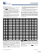
Table 9. Device Configuration and Control Latch Descriptions (continued)
Name Signal Description
[+] Feedback [+] Feedback