
Transceiver with Reclocker Specification Sheet


CYV15G0404DXB
Document #: 38-02097 Rev. *B Page 23 of 44
Device Configuration Strategy
The following is a series of ordered events needed to load the
configuration latches on a per channel basis:
1. Pulse RESET
Low after device power up. This operation
resets all four channels. Initialize the JTAG state machine to
its reset state as detailed in the JTAG Support section.
2. Set the static receiver latch bank for the target channel. May
be performed using a global operation, if the application
permits it. [Optional step if the default settings match the
desired configuration.]
3. Set the static transmitter latch bank for the target channel.
May be performed using a global operation, if the application
permits it. [Optional step if the default settings match the
desired configuration.]
4. Set the dynamic bank of latches for the target channel. Enable
the Receive PLLs and transmit channels. May be performed
using a global operation, if the application permits it.
[Required step.]
5. Reset the Phase Alignment Buffer for the target channel. May
be performed using a global operation, if the application
permits it. [Optional if phase align buffer is bypassed.]
When a receive channel is configured with the decoder
bypassed and the receive clock selected as recovered clock in
half rate mode (DECBYPx = 0, RXRATEx = 0, RXCKSELx = 0),
the channel cannot be dynamically reconfigured to enable the
decoder with RXCLKx selected as the REFCLKx (DECBYPx =
1, RXCKSELx = 1). If such a change is desired, a global reset
should be performed and all channels should be reconfigured to
the desired settings.
JTAG Support
The CYV15G0404DXB contains a JTAG port to allow system
level diagnosis of device interconnect. Of the available JTAG
modes, boundary scan, and bypass are supported. This
capability is present only on the LVTTL inputs and outputs and
the REFCLKx± clock input. The high-speed serial inputs and
outputs are not part of the JTAG test chain.
To ensure valid device operation after power up (including
non-JTAG operation),
the JTAG state machine must also be
initialized to a reset state. This is done in addition to the device
reset (using RESET)
. The JTAG state machine is initialized using
TRST
(asserting it LOW and de-asserting it or leaving it
asserted), or by asserting TMS HIGH for at least five consecutive
TCLK cycles. This is necessary to ensure that the JTAG
controller does not enter any of the test modes after device
power up. In this JTAG reset state, the rest of the device is in
normal operation.
Note. The order of device reset (using RESET
) and JTAG initial-
ization does not matter.
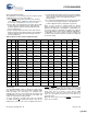
Table 10. Device Control Latch Configuration Table
ADDR Channel Type DATA7 DATA6 DATA5 DATA4 DATA3 DATA2 DATA1 DATA0
Reset
Value
0
(0000b)
A S RFMODEA[1] RFMODEA[0] FRAMCHARA DECMODEA DECBYPA RXCKSELA RXRATEA GLEN0 10111111
1
(0001b)
A S SDASEL2A[1] SDASEL2A[0] SDASEL1A[1] SDASEL1A[0] ENCBYPA TXCKSELA TXRATEA GLEN1 10101101
2
(0010b)
A D RFENA RXPLLPDA RXBISTA TXBISTA OE2A OE1A PABRSTA GLEN2 10110011
3
(0011b)
B S RFMODEB[1] RFMODEB[0] FRAMCHARB DECMODEB DECBYPB RXCKSELB RXRATEB GLEN3 10111111
4
(0100b)
B S SDASEL2B[1] SDASEL2B[0] SDASEL1B[1] SDASEL1B[0] ENCBYPB TXCKSELB TXRATEB GLEN4 10101101
5
(0101b)
B D RFENB RXPLLPDB RXBISTB TXBISTB OE2B OE1B PABRSTB GLEN5 10110011
6
(0110b)
C S RFMODEC[1] RFMODEC[0] FRAMCHARC DECMODEC DECBYPC RXCKSELC RXRATEC GLEN6 10111111
7
(0111b)
C S SDASEL2C[1] SDASEL2C[0] SDASEL1C[1] SDASEL1C[0] ENCBYPC TXCKSELC TXRATEC GLEN7 10101101
8
(1000b)
C D RFENC RXPLLPDC RXBISTC TXBISTC OE2C OE1C PABRSTC GLEN8 10110011
9
(1001b)
D S RFMODED[1] RFMODED[0] FRAMCHARD DECMODED DECBYPD RXCKSELD RXRATE D GLEN9 10111111
10
(1010b)
D S SDASEL2D[1] SDASEL2D[0] SDASEL1D[1] SDASEL1D[0] ENCBYPD TXCKSELD TXRATED GLEN10 10101101
11
(1011b)
D D RFEND RXPLLPDD RXBISTD TXBISTD OE2D OE1D PABRSTD GLEN11 10110011
12
(1100b)
GLOBAL S RFMODEGL[1] RFMODE
GL[0]
FRAMCHARGL DECMODEGL DECBYPGL RXCKSELGL RXRATEG
L
FGLEN0 N/A
13
(1101b)
GLOBAL S SDASEL2GL[1] SDASEL2GL[
0]
SDASEL1GL[1] SDASEL1GL[0
]
ENCBPGL TXCKSELGL TXRATEG
L
FGLEN1 N/A
14
(1110b)
GLOBAL D RFENGL RXPLLPDGL RXBISTGL TXBISTGL OE2GL OE1GL PABRSTG
L
FGLEN2 N/A
15
(1111b)
MASK D D7 D6 D5 D4 D3 D2 D1 D0 11111111
[+] Feedback [+] Feedback