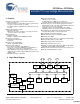
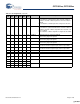
CY7C601xx, CY7C602xx enCoRe™ II Low Voltage Microcontroller 1.
CY7C601xx, CY7C602xx 3. Applications The CY7C601xx and CY7C602xx are targeted for the following applications: ■ PC wireless HID devices ❐ Mice (optomechanical, optical, trackball) ❐ Keyboards ❐ Presenter tools ■ Gaming ❐ Joysticks ❐ Gamepad ■ General purpose wireless applications ❐ Remote controls ❐ Barcode scanners ❐ POS terminal ❐ Consumer electronics ❐ Toys 4. Introduction The enCoRe II LV family brings the features and benefits of the enCoRe II to non USB applications.
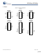
CY7C601xx, CY7C602xx 6. Pinouts Figure 6-1. Package Configurations Top View CY7C60223 24-Pin PDIP P3.0 P3.1 SCLK/P1.4 SMOSI/P1.5 SMISO/P1.6 P1.7 NC NC P0.7 TIO1/P0.6 TIO0/P0.5 INT2/P0.4 1 2 3 4 5 6 7 8 9 10 11 12 24 23 22 21 20 19 18 17 16 15 14 13 P1.3/SSEL P1.2 VDD P1.1 P1.0 VSS P2.0 P2.1 P0.0/CLKIN P0.1/CLKOUT P0.2/INT0 P0.3/INT1 CY7C60113 28-Pin SSOP VDD P2.7 P2.6 P2.5 P2.4 P0.7 TIO1/P0.6 TIO0/P0.5 INT2/P0.4 INT1/P0.3 INT0/P0.2 CLKOUT/P0.1 CLKIN/P0.
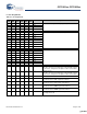
CY7C601xx, CY7C602xx 6.1 Pin Assignments Table 6-1. Pin Assignments 48 40 28 24 24 SSOP PDIP SSOP QSOP SOIC 24 PDIP Name Description 7 3 P4.0 6 2 P4.1 42 38 P4.2 43 39 P4.3 34 30 19 18 1 35 31 20 19 2 36 32 37 33 38 34 24 P3.4 39 35 25 P3.5 40 36 26 P3.6 41 37 27 P3.7 15 11 11 11 18 P2.0 14 10 10 10 17 P2.1 13 9 12 8 11 7 5 P2.4 10 6 4 P2.5 9 5 3 P2.6 8 4 2 P2.7 25 21 15 14 13 20 P1.
CY7C601xx, CY7C602xx Table 6-1. Pin Assignments (continued) 48 40 28 24 24 SSOP PDIP SSOP QSOP SOIC 24 PDIP Name Description 23 19 13 9 9 16 P0.0/CLKIN 22 18 12 8 8 15 P0.1/CLKOUT GPIO Port 0 bit 1—Configured individually On CY7C601xx, optional Clock Out when external oscillator is disabled or external oscillator output drive when external oscillator is enabled. On CY7C602xx, oscillator output when configured as Clock Out. 21 17 11 7 7 14 P0.
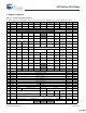
CY7C601xx, CY7C602xx 7. Register Summary Table 7-1. enCoRe II LV Register Summary The XIO bit in the CPU Flags Register must be set to access the extended register space for all registers above 0xFF. Addr Name 7 6 5 4 3 2 1 0 R/W Default 00 P0DATA P0.7 P0.6/TIO1 P0.5/TIO0 P0.4/INT2 P0.3/INT1 P0.2/INT0 P0.1/ CLKOUT P0.0/CLKIN bbbbbbbb 00000000 01 P1DATA P1.7 P1.4/SCLK P1.3/SSEL P1.2 P1.1 P1.0 bbbbbbbb 00000000 02 P2DATA P2.7–P2.2 P2.1–P2.
CY7C601xx, CY7C602xx Table 7-1. enCoRe II LV Register Summary (continued) The XIO bit in the CPU Flags Register must be set to access the extended register space for all registers above 0xFF.
CY7C601xx, CY7C602xx 8. CPU Architecture This family of microcontrollers is based on a high performance, 8-bit, Harvard architecture microprocessor. Five registers control the primary operation of the CPU core. These registers are affected by various instructions, but are not directly accessible through the register space by the user. Table 8-1.
CY7C601xx, CY7C602xx 9.1.1 Accumulator Register Table 9-2. CPU Accumulator Register (CPU_A) Bit # 7 6 5 Field 4 3 2 1 0 CPU Accumulator [7:0] Read/Write – – – – – – – – Default 0 0 0 0 0 0 0 0 Bit [7:0]: CPU Accumulator [7:0] 8-bit data value holds the result of any logical or arithmetic instruction that uses a source addressing mode. 9.1.2 Index Register Table 9-3.
CY7C601xx, CY7C602xx 9.2 Addressing Modes 9.2.1 Source Immediate 9.2.3 Source Indexed The result of an instruction using this addressing mode is placed in the A register, the F register, the SP register, or the X register, which is specified as part of the instruction opcode. Operand 1 is an immediate value that serves as a source for the instruction. Arithmetic instructions require two sources; the second source is the A, X, SP, or F register specified in the opcode.
CY7C601xx, CY7C602xx 9.2.5 Destination Indexed 9.2.7 Destination Indexed Source Immediate The result of an instruction using this addressing mode is placed within either the RAM memory space or the register space. Operand 1 is added to the X register forming the address that points to the location of the result. The source for the instruction is the A register. Arithmetic instructions require two sources; the second source is the location specified by Operand 1 added with the X register.
CY7C601xx, CY7C602xx 9.2.9 Source Indirect Post Increment 9.2.10 Destination Indirect Post Increment The result of an instruction using this addressing mode is placed in the Accumulator. Operand 1 is an address pointing to a location within the memory space, which contains an address (the indirect address) for the source of the instruction. The indirect address is incremented as part of the instruction execution. This addressing mode is only valid on the MVI instruction.
CY7C601xx, CY7C602xx 15 8 2 SUB [X+expr], A C, Z 16 9 3 1 Instruction Format Flags 6D 4 1 RRC A C, Z AND reg[expr], expr Z 6E 7 2 RRC [expr] C, Z 42 10 3 AND reg[X+expr], expr Z 6F 8 2 RRC [X+expr] C, Z OR reg[expr], expr Z 70 AND F, expr C, Z OR F, expr C, Z 9 3 3 NOP Bytes 41 Flags Cycles 40 4 C, Z Instruction Format Opcode Hex C, Z SUB [expr], A Bytes SUB A, [X+expr] 7 2 Flags Cycles 7 2 14 Instruction Format[1, 2] Opcode Hex Cycles 13 Bytes Opcode
CY7C601xx, CY7C602xx 11. Memory Organization 11.1 Flash Program Memory Organization Figure 11-1.
CY7C601xx, CY7C602xx 11.2 Data Memory Organization The CY7C601xx and CY7C602xx microcontrollers provide up to 256 bytes of data RAM Figure 11-2. Data Memory Organization After Reset Address 8-bit PSP 0x00 Top of RAM Memory Stack begins here and grows upward 0xFF 11.3 Flash 11.4 SROM This section describes the Flash block of enCoRe II LV. Much of the visible Flash functionality, including programming and security, are implemented in the M8C Supervisory Read Only Memory (SROM).
CY7C601xx, CY7C602xx Two important variables used for all functions are KEY1 and KEY2. These variables help discriminate between valid and inadvertent SSCs. KEY1 always has a value of 3Ah, while KEY2 has the same value as the stack pointer when the SROM function begins execution. This is the Stack Pointer value when the SSC opcode is executed, plus three. If either of the keys do not match the expected values, the M8C halts (with the exception of the SWBootReset function).
CY7C601xx, CY7C602xx Table 11-6. EraseBlock Parameters 11.5.3 WriteBlock Function The WriteBlock function is used to store data in Flash. Data is moved 64 bytes at a time from SRAM to Flash using this function. The WriteBlock function first checks the protection bits and determines if the desired BLOCKID is writable. If write protection is turned on, the WriteBlock function exits setting the accumulator and KEY2 back to 00h. KEY1 has a value of 01h, indicating a write failure.
CY7C601xx, CY7C602xx Table 11-8. ProtectBlock Parameters Name Address Description KEY1 0,F8h 3Ah KEY2 0,F9h Stack Pointer value when SSC is executed CLOCK 0,FCh Clock Divider used to set the write pulse width DELAY 0,FEh For a CPU speed of 12 MHz set to 56h 11.5.6 EraseAll Function The EraseAll function performs a series of steps that destroy the user data in the Flash macros and resets the protection block in each Flash macro to all zeros (the unprotected state).
CY7C601xx, CY7C602xx 11.6 SROM Table Read Description The Silicon IDs for enCoRe II LV devices are stored in SROM tables in the part, as shown in Figure 11-3. on page 20 The Silicon ID can be read out from the part using SROM Table reads. This is demonstrated in the following pseudo code. As mentioned in the section SROM on page 15, the SROM variables occupy address F8h through FFh in the SRAM. Each of the variables and their definition are given in the section SROM on page 15.
CY7C601xx, CY7C602xx Figure 11-3. SROM Table F8h F9h Silicon ID [15-8] Silicon ID [7-0] Table 1 Family / Die ID Revision ID FBh Table 2 32 KHz 32 KHz FCh FDh 24 MHz IOSCTR at 3.30V 24 MHz IOSCTR at 3.00V FEh FFh lid in g Va rat n pe i o O Re g Table 0 FAh 32 KHz 24 MHz IOSCTR at 2.85V 24 MHz IOSCTR at 2.70V 32 KHz Table 3 LPOSCTR LPOSCTR LPOSCTR LPOSCTR at 3.30V at 3.00V at 2.85V at 2.70V Table 4 Table 5 Table 6 Table 7 11.6.
CY7C601xx, CY7C602xx 12. Clocking The enCoRe II LV has two internal oscillators, the internal 24 MHz oscillator and the 32 kHz low power oscillator. The internal 24 MHz oscillator is designed such that it is trimmed to an output frequency of 24 MHz over temperature and voltage variation. The internal 24 MHz oscillator accuracy is 24 MHz –22% to +10% (between 0° and 70°C). No external components are required to achieve this level of accuracy.
CY7C601xx, CY7C602xx When using the 32 kHz oscillator, the PITMRL/H is read until two consecutive readings match before sending and receiving data. The following firmware example assumes the developer is interested in the lower byte of the PIT. 12.
CY7C601xx, CY7C602xx Figure 12-1. CPU Clock Block Diagram XOSC SEL EN P0.1 CLKOUT XTAL OSC 1-24MHz P0.0 CLKIN EFTB CLK_EXT MUX CY7C601xx only CY7C601xx only Crystal Oscillator Disabled LP OSC 32-KHz CLK_32KHz CPUCLK SEL CLK_EXT SCALE (divide by 2n, n = 0-5,7) CLK_CPU Doubler CLK_HS MUX CLK_24MHz Table 12-2.
CY7C601xx, CY7C602xx Table 12-3. OSC Control 0 (OSC_CR0) [0x1E0] [R/W] (continued) Read/Write – – R/W R/W R/W R/W R/W R/W Default 0 0 0 0 0 0 0 0 Bit [7:6]: Reserved Bit 5: No Buzz During sleep (the Sleep bit is set in the CPU_SCR Register—Table 13-1), the LVD and POR detection circuit is turned on periodically to detect any POR and LVD events on the VCC pin (the Sleep Duty Cycle bits in the ECO_TR are used to control the duty cycle—Table 15-3).
CY7C601xx, CY7C602xx Table 12-4. Clock IO Configuration (CLKIOCR) [0x32] [R/W] Bit # 7 6 5 Reserved Field 4 3 2 XOSC Select XOSC Enable EFTB Disabled 1 0 CLKOUT Select Read/Write – – – R/W R/W R/W R/W R/W Default 0 0 0 0 0 0 0 0 Bit [7:5]: Reserved Bit 4: XOSC Select This bit, when set, selects the external crystal oscillator clock as clock source of external clock. When selecting the crystal oscillator clock, first enable the crystal oscillator and wait for few cycles.
CY7C601xx, CY7C602xx Figure 12-2. Programmable Interval Timer Block Diagram System Clock Configuration Status and Control 12-bit reload value 12-bit down counter Clock Timer 12-bit reload control Interrupt Controller 12.2.3 Timer Capture Clock (TCAPCLK) The Timer Capture clock (TCAPCLK) is sourced from the external crystal oscillator, the internal 24 MHz oscillator or the internal 32 kHz low power oscillator. A programmable prescaler of 2, 4, 6, or 8 then divides the selected source. Figure 12-3.
CY7C601xx, CY7C602xx Table 12-5. Timer Clock Configuration (TMRCLKCR) [0x31] [R/W] Bit # 7 Field TCAPCLK Divider 6 5 4 TCAPCLK Select 3 2 1 ITMRCLK Divider 0 ITMRCLK Select Read/Write R/W R/W R/W R/W R/W R/W R/W R/W Default 1 0 0 0 1 1 1 1 Bit [7:6]: TCAPCLK Divider [1:0] TCAPCLK Divider controls the TCAPCLK divisor.
CY7C601xx, CY7C602xx 12.2.4 Internal Clock Trim Table 12-6. IOSC Trim (IOSCTR) [0x34] [R/W] Bit # 7 6 Field 5 4 3 foffset[2:0] 2 1 0 Gain[4:0] Read/Write R/W R/W R/W R/W R/W R/W R/W R/W Default 0 0 0 D D D D D The IOSC Calibrate Register is used to calibrate the internal oscillator. The reset value is undefined, but during boot the SROM writes a calibration value that is determined during manufacturing test. The ‘D’ indicates that the default value is trimmed to 24 MHz at 3.
CY7C601xx, CY7C602xx 12.2.6 LPOSC Trim Table 12-8. LPOSC Trim (LPOSCTR) [0x36] [R/W] Bit # 7 6 Field 32 kHz Low Power Reserved 5 4 3 Read/Write R/W – R/W R/W R/W R/W R/W R/W Default 0 – D D D D D D 32 kHz Bias Trim [1:0] 2 1 0 32 kHz Freq Trim [3:0] This register is used to calibrate the 32 kHz low speed oscillator. The reset value is undefined but during boot the SROM writes a calibration value that is determined during manufacturing test.
CY7C601xx, CY7C602xx 13. Reset The microcontroller supports two types of resets: Power on Reset (POR) and Watchdog Reset (WDR). When reset is initiated, all registers are restored to their default states and all interrupts are disabled. The occurrence of a reset is recorded in the System Status and Control Register (CPU_SCR). Bits within this register record the occurrence of POR and WDR Reset respectively. The firmware interrogates these bits to determine the cause of a reset.
CY7C601xx, CY7C602xx 13.1 Power On Reset POR occurs every time the power to the device is switched on. POR is released when the supply is typically 2.6V for the upward supply transition, with typically 50 mV of hysteresis during the power on transient. Bit 4 of the System Status and Control Register (CPU_SCR) is set to record this event (the register contents are set to 00010000 by the POR).
CY7C601xx, CY7C602xx 14.1 Sleep Sequence 14.1.1 Low Power in Sleep Mode The SLEEP bit is an input into the sleep logic circuit. This circuit is designed to sequence the device into and out of the hardware sleep state. The hardware sequence to put the device to sleep is shown in Figure 14-1. and is defined as follows. 1. Firmware sets the SLEEP bit in the CPU_SCR0 register. The Bus Request (BRQ) signal to the CPU is immediately asserted.
CY7C601xx, CY7C602xx 14.2 Wakeup Sequence When asleep, the only event that wakes the system up is an interrupt. The global interrupt enable of the CPU flag register need not be set. Any unmasked interrupt wakes the system up. It is optional for the CPU to actually take the interrupt after the wakeup sequence.
CY7C601xx, CY7C602xx 15. Low Voltage Detect Control Table 15-1. Low Voltage Control Register (LVDCR) [0x1E3] [R/W] Bit # 7 Field 6 5 Reserved 4 PORLEV[1:0] 3 2 Reserved 1 0 VM[2:0] Read/Write – – R/W R/W – R/W R/W R/W Default 0 0 0 0 0 0 0 0 This register controls the configuration of the Power on Reset and Low Voltage Detection circuit. This register is accessed only in the second bank of IO space. This requires setting the XIO bit in the CPU flags register.
CY7C601xx, CY7C602xx 15.1 POR Compare State Table 15-2. Voltage Monitor Comparators Register (VLTCMP) [0x1E4] [R] Bit # 7 6 5 Field 4 3 2 Reserved 1 0 LVD PPOR Read/Write – – – – – – R R Default 0 0 0 0 0 0 0 0 This read-only register allows reading the current state of the LVD and PPOR comparators.
CY7C601xx, CY7C602xx 16. General Purpose IO Ports 16.1 Port Data Registers 16.1.1 P0 Data Table 16-1. P0 Data Register (P0DATA)[0x00] [R/W] Bit # 7 6 5 4 3 2 1 0 Field P0.7 P0.6/TIO1 P0.5/TIO0 P0.4/INT2 P0.3/INT1 P0.2/INT0 P0.1/CLKOUT P0.0/CLKIN Read/Write R/W R/W R/W R/W R/W R/W R/W R/W Default 0 0 0 0 0 0 0 0 This register contains the data for Port 0. Writing to this register sets the bit values to be output on output enabled pins.
CY7C601xx, CY7C602xx 16.1.3 P2 Data Table 16-3. P2 Data Register (P2DATA) [0x02] [R/W] Bit # 7 6 5 Field 4 3 2 1 P2.7–P2.2 0 P2.1–P2.0 Read/Write R/W R/W R/W R/W R/W R/W R/W R/W Default 0 0 0 0 0 0 0 0 This register contains the data for Port 2. Writing to this register sets the bit values to be output on output enabled pins. Reading from this register returns the current state of the Port 2 pins. Bit [7:2]: P2 Data [7:2] Bit [1:0]: P2 Data [1:0] 16.1.4 P3 Data Table 16-4.
CY7C601xx, CY7C602xx 16.2.4 High Sink 16.2.7 Output Enable When set, the output sinks up to 50 mA. When set, the output driver of the pin is enabled. When clear, the output sinks up to 8 mA. When clear, the output driver of the pin is disabled. On the CY7C601xx, only the P3.7, P2.7, P0.1, and P0.0 have 50 mA sink drive capability. Other pins have 8 mA sink drive capability. For pins with shared functions there are some special cases. P0.0(CLKIN) and P0.
CY7C601xx, CY7C602xx 16.2.10 P0.1/CLKOUT Configuration Table 16-7. P0.1/CLKOUT Configuration (P01CR) [0x06] R/W] Bit # 7 6 5 4 3 2 1 0 Field CLK Output Int Enable Int Act Low TTL Thresh High Sink Open Drain Pull up Enable Output Enable Read/Write R/W R/W R/W R/W R/W R/W R/W R/W Default 0 0 0 0 0 0 0 0 This pin is shared between the P0.1 GPIO use and the CLKOUT pin for the external crystal oscillator.
CY7C601xx, CY7C602xx 16.2.12 P0.5/TIO0–P0.6/TIO1 Configuration Table 16-9. P0.5/TIO0–P0.6/TIO1 Configuration (P05CR–P06CR) [0x0A–0x0B] [R/W] Bit # 7 6 5 4 3 2 1 0 Field TIO Output Int Enable Int Act Low TTL Thresh Reserved Open Drain Pull up Enable Output Enable Read/Write R/W R/W R/W R/W – R/W R/W R/W Default 0 0 0 0 0 0 0 0 These registers control the operation of pins P0.5 through P0.6, respectively. P0.5 and P0.6 are shared with TIO0 and TIO1 respectively.
CY7C601xx, CY7C602xx 16.2.15 P1.1 Configuration Table 16-12. P1.1 Configuration (P11CR) [0x0E] [R/W] Bit # 7 6 5 Field Reserved Int Enable Int Act Low 4 3 Read/Write – R/W R/W – – Default 0 0 0 0 0 Reserved 2 1 0 Open Drain Reserved Output Enable R/W – R/W 0 0 0 This register controls the operation of the P1.1 pin. The pull up resistor on this pin is enabled by the P10CR Register. Note There is no 2 mA sourcing capability on this pin.
CY7C601xx, CY7C602xx 16.2.18 P1.4–P1.6 Configuration (SCLK, SMOSI, SMISO) Table 16-15. P1.4–P1.6 Configuration (P14CR–P16CR) [0x11–0x13] [R/W] Bit # 7 6 5 4 3 2 1 0 Field SPI Use Int Enable Int Act Low Reserved High Sink Open Drain Pull Up Enable Output Enable Read/Write R/W R/W R/W – R/W R/W R/W R/W Default 0 0 0 0 0 0 0 0 These registers control the operation of pins P1.4–P1.6, respectively. These registers exist in all enCoRe II LV parts.
CY7C601xx, CY7C602xx 16.2.21 P3 Configuration Table 16-18. P3 Configuration (P3CR) [0x16] [R/W] Bit # 7 6 5 4 3 2 1 0 Field Reserved Int Enable Int Act Low TTL Thresh High Sink Open Drain Pull Up Enable Output Enable Read/Write – R/W R/W R/W R/W R/W R/W R/W Default 0 0 0 0 0 0 0 0 In CY7C602xx, this register controls the operation of pins P3.0–P3.1. In CY7C601xx, this register controls the operation of pins P3.0–P3.7.
CY7C601xx, CY7C602xx 17. Serial Peripheral Interface (SPI) The SPI Master and Slave Interface core logic runs on the SPI clock domain. The SPI clock is a divider off of the CPUCLK when in Master Mode. SPI is a four pin serial interface comprised of a clock, an enable, and two data pins. Figure 17-1.
CY7C601xx, CY7C602xx 17.1 SPI Data Register Table 17-1. SPI Data Register (SPIDATA) [0x3C] [R/W] Bit # 7 6 5 4 Field 3 2 1 0 SPIData[7:0] Read/Write R/W R/W R/W R/W R/W R/W R/W R/W Default 0 0 0 0 0 0 0 0 When read, this register returns the contents of the receive buffer. When written, it loads the transmit holding register.
CY7C601xx, CY7C602xx Table 17-3. SPI Mode Timing vs.
CY7C601xx, CY7C602xx Table 17-4. SPI SCLK Frequency SCLK CPUCLK Select Divisor SCLK Frequency when CPUCLK = 12 MHz 00 6 2 MHz 01 12 1 MHz 10 48 250 kHz 11 96 125 kHz 17.3 SPI Interface Pins The SPI interface uses the P1.3–P1.6 pins. These pins are configured using the P1.3 and P1.4–P1.6 configuration. 18. Timer Registers All timer functions of the enCoRe II LV are provided by a single timer block. The timer block is asynchronous from the CPU clock.
CY7C601xx, CY7C602xx Table 18-2. Free Running Timer High Order Byte (FRTMRH) [0x21] [R/W] Bit # 7 6 5 Field 4 3 2 1 0 Free Running Timer [15:8] Read/Write R/W R/W R/W R/W R/W R/W R/W R/W Default 0 0 0 0 0 0 0 0 Bit [7:0]: Free Running Timer [15:8] When reading the free running timer, the low order byte is read first and the high order second. When writing, the low order byte is written first, then the high order byte. 18.1.2 Time Capture enCoRe II LV has two 8-bit captures.
CY7C601xx, CY7C602xx Table 18-4.
CY7C601xx, CY7C602xx Table 18-8. Timer Capture 1 Falling (TCAP1F) [0x25] [R/W] Bit # 7 6 5 Field 4 3 2 1 0 Capture 1 Falling [7:0] Read/Write R R R R R R R R Default 0 0 0 0 0 0 0 0 Bit [7:0]: Capture 1 Falling [7:0] This register holds the value of the free running timer when the last falling edge occurred on the TIO1 input. The bits stored here are selected by the Prescale [2:0] bits in the Timer Configuration register.
CY7C601xx, CY7C602xx Table 18-11. Programmable Interval Timer High (PITMRH) [0x27] [R] Bit # 7 6 Field 5 4 3 Reserved 2 1 0 Prog Interval Timer [11:8] Read/Write -- -- -- -- R R R R Default 0 0 0 0 0 0 0 0 Bit [7:4]: Reserved Bit [3:0]: Prog Internal Timer [11:8] This register holds the high order nibble of the 12-bit programmable interval timer. Reading this register returns the high order nibble of the 12-bit timer at the instant when the low order byte was last read.
CY7C601xx, CY7C602xx Figure 18-3. Timer Functional Sequence Diagram Document 38-16016 Rev.
CY7C601xx, CY7C602xx Figure 18-4. 16-Bit Free Running Counter Loading Timing Diagram clk_sys write valid addr write data FRT reload ready Clk Timer 12b Prog Timer 12b reload interrupt 12-bit programmable timer load timing Capture timer clk 16b free running counter load 16b free running counter 00A0 00A1 00A2 00A3 00A4 00A5 00A6 00A7 00A8 00A9 00AB 00AC 00AD 00AE 00AF 00B0 00B1 00B2 ACBE ACBF ACC0 16-bit free running counter loading timing Figure 18-5.
CY7C601xx, CY7C602xx 19. Interrupt Controller Table 19-1. Interrupt Priorities, Address, and Name (contin- The interrupt controller and its associated registers allow the user’s code to respond to an interrupt from almost every functional block in the enCoRe II LV devices. The registers associated with the interrupt controller are disabled either globally or individually.
CY7C601xx, CY7C602xx 19.2 Interrupt Processing The sequence of events that occur during interrupt processing is as follows: 1. An interrupt becomes active, either because: a. The interrupt condition occurs (for example, a timer expires). b. A previously posted interrupt is enabled through an update of an interrupt mask register. c. An interrupt is pending and GIE is set from 0 to 1 in the CPU Flag register. 2. The current executing instruction finishes. 3.
CY7C601xx, CY7C602xx Table 19-3. Interrupt Clear 1 (INT_CLR1) [0xDB] [R/W] Bit # 7 6 5 Field TCAP0 Prog Interval Timer 1-ms Programmable Interrupt 4 3 Read/Write R/W R/W R/W – – Default 0 0 0 0 0 2 1 0 – – – 0 0 0 Reserved When reading this register, 0 = There is no posted interrupt for the corresponding hardware. 1 = There is a posted interrupt for the corresponding hardware. Writing a ‘0’ to the bits clears the posted interrupts for the corresponding hardware.
CY7C601xx, CY7C602xx Table 19-6.
CY7C601xx, CY7C602xx Table 19-8.
CY7C601xx, CY7C602xx 20. Absolute Maximum Ratings Maximum Total Sink Output Current into Port 0 and 1 and Pins............................................................. 70 mA Storage Temperature ................................... –40°C to +90°C Maximum Total Source Output Current into GPIO Pins30 mA Ambient Temperature with Power Applied..... –0°C to +70°C Supply Voltage on VCC Relative to VSS ..........–0.5V to +7.0V Maximum On-chip Power Dissipation on any GPIO Pin...............................
CY7C601xx, CY7C602xx 20.2 AC Characteristics Parameter Description Conditions Min Typical Max Unit Clock TECLKDC External Clock Duty Cycle 45 55 % TECLK2 External Clock Frequency 1 24 MHz FIMO Internal Main Oscillator Frequency With proper trim values loaded[5] 18.72 26.4 MHz FILO Internal Low Power Oscillator With proper trim values loaded[5] 15.0001 50.
CY7C601xx, CY7C602xx Figure 20-2. GPIO Timing Diagram 90% GPIO Pin Output Voltage 10% TR_GPIO TF_GPIO Figure 20-3. SPI Master Timing, CPHA = 1 SS (SS is under firmware control in SPI Master mode) TSCKL SCK (CPOL=0) TSCKH SCK (CPOL=1) TMDO MSB MOSI MISO MSB LSB LSB TMSU TMHD Document 38-16016 Rev.
CY7C601xx, CY7C602xx Figure 20-4. SPI Slave Timing, CPHA = 1 SS TSSS TSSH TSCKL SCK (CPOL=0) TSCKH SCK (CPOL=1) MOSI MSB LSB TSSU TSHD TSDO MSB MISO LSB Figure 20-5. SPI Master Timing, CPHA = 0 SS (SS is under firmware control in SPI Master mode) TSCKL SCK (CPOL=0) TSCKH SCK (CPOL=1) TMDO TMDO1 MSB MOSI MISO MSB LSB LSB TMSU TMHD Document 38-16016 Rev.
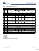
CY7C601xx, CY7C602xx Figure 20-6. SPI Slave Timing, CPHA = 0 SS TSSH TSSS TSCKL SCK (CPOL=0) TSCKH SCK (CPOL=1) MSB MOSI LSB TSSU TSHD TSDO TSDO1 MISO MSB LSB 1 21. Ordering Information Ordering Code FLASH Size RAM Size Package Type CY7C60123-PVXC 8K 256 48-SSOP CY7C60123-PXC 8K 256 40-PDIP CY7C60113-PVXC 8K 256 28-SSOP CY7C60223-PXC 8K 256 24-PDIP CY7C60223-SXC 8K 256 24-SOIC CY7C60223-QXC 8K 256 24-QSOP 22.
CY7C601xx, CY7C602xx 23. Package Diagrams Figure 23-1. 24-Pin (300-Mil) SOIC S13 NOTE : 1. JEDEC STD REF MO-119 PIN 1 ID 2. BODY LENGTH DIMENSION DOES NOT INCLUDE MOLD PROTRUSION/END FLASH,BUT DOES INCLUDE MOLD MISMATCH AND ARE MEASURED AT THE MOLD PARTING LINE. 12 1 MOLD PROTRUSION/END FLASH SHALL NOT EXCEED 0.010 in (0.254 mm) PER SIDE 3. DIMENSIONS IN INCHES MIN. MAX. 4. PACKAGE WEIGHT 0.65gms 0.291[7.391] 0.300[7.620] * 0.394[10.007] 0.419[10.642] 13 24 PART # S24.3 STANDARD PKG. SZ24.
CY7C601xx, CY7C602xx Figure 23-3. 24-Pin QSOP O241 0.033 REF. 12 0.228 1 PIN 1 ID 0.150 0.157 DIMENSIONS IN INCHES MIN. MAX. 0.244 13 24 0.337 0.344 SEATING PLANE 0.007 0.010 0.053 0.069 0.004 0.004 0.010 0.008 0.012 0.016 0.034 0.025 BSC. 0°-8° 51-85055-*B Figure 23-4. 28-Pin (5.3 mm) Shrunk Small Outline Package O28 51-85079-*C Document 38-16016 Rev.
CY7C601xx, CY7C602xx Figure 23-5. 40-Pin (600-Mil) Molded DIP P17 51-85019-*A Figure 23-6. 48-Pin Shrunk Small Outline Package O48 51-85061-*C Document 38-16016 Rev.
CY7C601xx, CY7C602xx 24. Document History Page Document Title: CY7C601xx, CY7C602xx enCoRe™ II Low Voltage Microcontroller Document Number: 38-16016 Rev. ECN Orig.
CY7C601xx, CY7C602xx Sales, Solutions, and Legal Information Worldwide Sales and Design Support Cypress maintains a worldwide network of offices, solution centers, manufacturer’s representatives, and distributors. To find the office closest to you, visit us at cypress.com/sales. Products PSoC Clocks & Buffers PSoC Solutions psoc.cypress.com clocks.cypress.com General Low Power/Low Voltage psoc.cypress.com/solutions psoc.cypress.com/low-power Wireless wireless.cypress.