
Low Voltage Microcontroller Specification Sheet


CY7C601xx, CY7C602xx
Document 38-16016 Rev. *E Page 36 of 68
16. General Purpose IO Ports
16.1 Port Data Registers
16.1.1 P0 Data
16.1.2 P1 Data
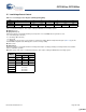
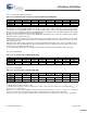
Table 16-1. P0 Data Register (P0DATA)[0x00] [R/W]
Bit # 7 6 5 4 3 2 1 0
Field P0.7 P0.6/TIO1 P0.5/TIO0 P0.4/INT2 P0.3/INT1 P0.2/INT0 P0.1/CLKOUT P0.0/CLKIN
Read/Write R/W R/W R/W R/W R/W R/W R/W R/W
Default 0 0 0 0 000 0
This register contains the data for Port 0. Writing to this register sets the bit values to be output on output enabled pins. Reading
from this register returns the current state of the Port 0 pins.
Bit 7: P0.7 Data
Bit [6:5]: P0.6–P0.5 Data/TIO1 and TIO0
Beside their use as the P0.6–P0.5 GPIOs, these pins are also used for alternate functions as the Capture Timer input or timer
output pins (TIO1 and TIO0). To configure the P0.5 and P0.6 pins, refer to the P0.5/TIO0–P0.6/TIO1 Configuration Register
(Table 16 -9).
Bit [4:2]: P0.4–P0.2 Data/INT2–INT0
Beside their use as the P0.4–P0.2 GPIOs, these pins are also used for the alternate functions as the interrupt pins (INT0–INT2).
To configure the P0.4–P0.2 pins, refer to the P0.2/INT0–P0.4/INT2 Configuration Register (Table 16-8).
Bit 1: P0.1/CLKOUT
Beside its use as the P0.1 GPIO, this pin is also used for the alternate function as the CLK OUT pin. To configure the P0.1 pin,
refer to the P0.1/CLKOUT Configuration Register (Table 16-7).
Bit 0: P0.0/CLKIN
Beside its use as the P0.0 GPIO, this pin is also used for the alternate function as the CLKIN pin. To configure the P0.0 pin, refer
to the P0.0/CLKIN Configuration Register (Table 16-6).
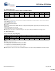
Table 16-2. P1 Data Register (P1DATA) [0x01] [R/W]
Bit # 7 6 5 4 3 2 1 0
Field P1.7 P1.6/SMISO P1.5/SMOSI P1.4/SCLK P1.3/SSEL P1.2 P1.1 P1.0
Read/Write R/W R/W R/W R/W R/W R/W R/W R/W
Default 0 0 0 0 0 0 0 0
This register contains the data for Port 1. Writing to this register sets the bit values to be output on output enabled pins. Reading
from this register returns the current state of the Port 1 pins.
Bit 7: P1.7 Data
Bit [6:3]: P1.6–P1.3 Data/SPI Pins (SMISO, SMOSI, SCLK, SSEL)
Beside their use as the P1.6–P1.3 GPIOs, these pins are also used for the alternate function as the SPI interface pins. To
configure the P1.6–P1.3 pins, refer to the P1.3–P1.6 Configuration Register (Table 16-14).
Bit [2:0]: P1.2–P1.0
[+] Feedback [+] Feedback