
Low Voltage Microcontroller Specification Sheet

CY7C601xx, CY7C602xx
Document 38-16016 Rev. *E Page 42 of 68
16.2.18 P1.4–P1.6 Configuration (SCLK, SMOSI, SMISO)
16.2.19 P1.7 Configuration
16.2.20 P2 Configuration
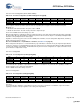
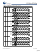
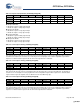
Table 16-15. P1.4–P1.6 Configuration (P14CR–P16CR) [0x11–0x13] [R/W]
Bit # 7 6 5 4 3 2 1 0
Field SPI Use Int Enable Int Act Low Reserved High Sink Open Drain Pull Up Enable Output Enable
Read/Write R/W R/W R/W –R/WR/WR/W R/W
Default 0 0 0 0000 0
These registers control the operation of pins P1.4–P1.6, respectively. These registers exist in all enCoRe II LV parts.
Bit 7: SPI Use
0 = Disable the SPI alternate function. The pin is used as a GPIO
1 = Enable the SPI function. The SPI circuitry controls the output of the pin
The P1.4–P1.6 GPIO’s threshold is always set to TTL.
When the SPI hardware is enabled, pins that are configured as SPI Use have their output enable and output state controlled by
the SPI circuitry. When the SPI hardware is disabled or a pin has its SPI Use bit clear, the pin is controlled by the Output Enable
bit and the corresponding bit in the P1 data register.
Regardless of whether any pin is used as an SPI or GPIO pin the Int Enable, Int act Low, High Sink, Open Drain, and Pull up
Enable control the behavior of the pin.
Note for Comm Modes 01 or 10 (SPI Master or SPI Slave, see Table 17-2 on page 45)
When configured for SPI (SPI Use = 1 and Comm Modes [1:0] = SPI Master or SPI Slave mode), the input and output direction
of pins P1.5, and P1.6 is set automatically by the SPI logic. However, pin P1.4's input and output direction is NOT automatically
set; it must be explicitly set by firmware. For SPI Master mode, pin P1.4 must be configured as an output; for SPI Slave mode,
pin P1.4 must be configured as an input.
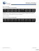
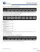
Table 16-16. P1.7 Configuration (P17CR) [0x14] [R/W]
Bit # 7 6 5 4 3 2 1 0
Field Reserved Int Enable Int Act Low Reserved High Sink Open Drain Pull Up Enable Output Enable
Read/Write –R/WR/W–R/W R/W R/W R/W
Default 00000000
This register controls the operation of pin P1.7.
The 50 mA sink drive capability is only available in CY7C602xx. In CY7C601xx, only 8 mA sink drive capability is available on
this pin regardless of the setting of the High Sink bit.
The P1.7 GPIO’s threshold is always set to TTL.
Table 16-17. P2 Configuration (P2CR) [0x15] [R/W]
Bit # 7 6 5 4 3 2 1 0
Field Reserved Int Enable Int Act Low TTL Thresh High Sink Open Drain Pull Up Enable Output Enable
Read/Write –R/WR/WR/WR/W R/W R/W R/W
Default 00000000
In CY7C602xx, this register controls the operation of pins P2.0–P2.1. In CY7C601xx, this register controls the operation of pins
P2.0–P2.7.
The 50 mA sink drive capability is only available on pin P2.7 and only on CY7C601xx. In CY7C602xx, only 8 mA sink drive
capability is available on this pin regardless of the setting of the High Sink bit.
[+] Feedback [+] Feedback