
Low Voltage Microcontroller Specification Sheet

CY7C601xx, CY7C602xx
Document 38-16016 Rev. *E Page 43 of 68
16.2.21 P3 Configuration
16.2.22 P4 Configuration
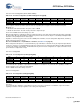
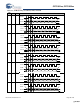
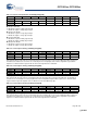
Table 16-18. P3 Configuration (P3CR) [0x16] [R/W]
Bit # 7 6 5 4 3 2 1 0
Field Reserved Int Enable Int Act Low TTL Thresh High Sink Open Drain Pull Up Enable Output Enable
Read/Write –R/WR/WR/WR/W R/W R/W R/W
Default 00000000
In CY7C602xx, this register controls the operation of pins P3.0–P3.1. In CY7C601xx, this register controls the operation of pins
P3.0–P3.7.
The 50 mA sink drive capability is only available on pin P3.7 and only on CY7C601xx. In CY7C602xx, only 8 mA sink drive
capability is available on this pin regardless of the setting of the High Sink bit.
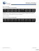
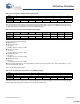
Table 16-19. P4 Configuration (P4CR) [0x17] [R/W]
Bit # 7 6 5 4 3 2 1 0
Field Reserved Int Enable Int Act Low TTL Thresh High Sink Open Drain Pull Up Enable Output Enable
Read/Write – R/W R/W R/W R/W R/W R/W R/W
Default 0 0 0 0 0 0 0 0
This register exists only in CY7C601xx. This register controls the operation of pins P4.0–P4.3.
[+] Feedback [+] Feedback