
Low Voltage Microcontroller Specification Sheet

CY7C601xx, CY7C602xx
Document 38-16016 Rev. *E Page 44 of 68
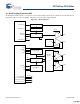
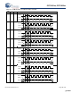
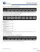
17. Serial Peripheral Interface (SPI)
The SPI Master and Slave Interface core logic runs on the SPI clock domain. The SPI clock is a divider off of the CPUCLK when in
Master Mode. SPI is a four pin serial interface comprised of a clock, an enable, and two data pins.
Figure 17-1. SPI Block Diagram
SPI State Machine
SS_N
Data (8 bit)
Load
Empty
Data (8 bit)
Load
Full
Sclk Output Enable
Slave Select Output Enable
Master IN, Slave Out OE
Master Out, Slave In, OE
Shift Buffer
Input Shift Buffer
Output Shift Buffer
SCK Clock Generation
SCK Clock Select
SCK Clock Phase/Polarity
Select
Register Block
SCK Speed Sel
Master/Slave Sel
SCK Polarity
SCK Phase
Little Endian Sel
MISO/MOSI
Crossbar
GPIO Block
SS_N
LE_SEL
SCK
LE_SEL
SCK_OE
SS_N_OE
MISO_OE
MOSI_OE
SCK
SCK_OE
SS_N_OE
SCK
SS_N
Master/Slave Set
MISO
MOSI
MISO_OE
MOSI_OE
[+] Feedback [+] Feedback