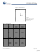
CY7C63310, CY7C638xx enCoRe™ II Low Speed USB Peripheral Controller 1. Features ■ USB 2.0-USB-IF certified (TID # 40000085) ■ enCoRe™ II USB - “enhanced Component Reduction” ❐ ■ ■ ■ ■ ■ ■ ❐ Two internal 3.3V regulators and an internal USB pull up resistor ❐ Configurable IO for real world interface without external components USB Specification compliance ■ 125 mA 3.3V voltage regulator powers external 3.3V devices ■ 3.3V IO pins ■ ❐ 4 IO pins with 3.3V logic levels ❐ Each 3.
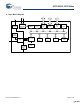
CY7C63310, CY7C638xx 2. Logic Block Diagram 3.3V Regulator Low-Speed USB/PS2 Transceiver and Pull up Low-Speed USB SIE Interrupt Control 4 3VIO/SPI Pins Up to 14 Extended IO Pins Up to 6 GPIO pins Wakeup Timer Internal 24 MHz Oscillator M8C CPU Clock Control RAM Up to 256 Byte Flash Up to 8K Byte 12-bit Timer 16-bit Free running timer External Clock Watchdog Timer Vdd POR / Low-Voltage Detect Document 38-08035 Rev.
CY7C63310, CY7C638xx 3. Introduction Cypress has reinvented its leadership position in the low speed USB market with a new family of innovative microcontrollers. Introducing enCoRe II USB - “enhanced Component Reduction.” Cypress has leveraged its design expertise in USB solutions to advance its family of low speed USB microcontrollers, which enable peripheral developers to design new products with a minimum number of components. The enCoRe II USB technology builds on the enCoRe family.
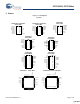
CY7C63310, CY7C638xx 5. Pinouts Figure 5-1. Pin Diagrams Top View CY7C63801, CY7C63310 16-Pin PDIP P1.2 VCC P1.1/D– P1.0/D+ VSS P0.0 P0.1 P0.2/INT0 TIO1/P0.6 TIO0/P0.5 INT2/P0.4 INT1/P0.3 INT0/P0.2 P0.1 P0.0 VSS 1 2 3 4 5 6 7 8 16 15 14 13 12 11 10 9 CY7C63813 18-Pin PDIP P1.2/VREG VCC P1.1/D– P1.0/D+ VSS P0.0 P0.1 P0.2/INT0 P0.3/INT1 P0.7 TIO1/P0.6 TIO0/P0.5 INT2/P0.4 INT1/P0.3 INT0/P0.2 P0.1 P0.0 VSS CY7C63823 24-Pin QSOP P1.7 P1.6/SMISO P1.5/SMOSI P1.4/SCLK P3.1 P3.0 P1.3/SSEL P1.2/VREG VCC P1.
CY7C63310, CY7C638xx Figure 5-2. CY7C63823 Die Form 23 1 22 Cypress Logo 21 2 20 3 19 4 18 17 Y 16 15 X 14 5 6 7 13 8 9 12 10 11 Legend Die step = 1792.98 μm x 2272.998 μm Die size = 1727 μm x 2187 μm Bond pad opening = 70 μm x 70 μm Die thickness = 14 mils Table 5-1. Die Pad Summary X (microns) Y (microns) 1 Pad Number P0.7 Pad Name -742.730 911.990 2 P0.6 -755.060 792.200 3 P0.5 -755.060 699.300 4 P0.4 -755.060 606.400 5 P0.3 -755.060 -430.080 6 P0.2 -755.
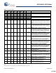
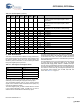
CY7C63310, CY7C638xx Table 5-2. Pin Description 32 QFN 24 QSOP 24 SOIC 21 19 18 P3.0 22 20 19 P3.1 9 11 11 P2.0 8 10 10 P2.1 14 14 13 10 15 9 13 P1.0/D+ GPIO Port 1 bit 0/USB D+ [1] If this pin is used as a General Purpose output, it draws current. This pin must be configured as an input to reduce current draw. 15 15 14 11 16 10 14 P1.1/D– GPIO Port 1 bit 1/USB D– [1] If this pin is used as a General Purpose output, it draws current.
CY7C63310, CY7C638xx Table 5-2. Pin Description (continued) 32 QFN 24 QSOP 24 SOIC 18 SIOC 18 PDIP 16 SOIC 16 PDIP 2 4 4 3 8 2 6 P0.5/TIO0 GPIO Port 0 bit 5. Configured individually Alternate function Timer capture inputs or Timer output TIO0 1 3 3 2 7 1 5 P0.6/TIO1 GPIO Port 0 bit 6. Configured individually Alternate function Timer capture inputs or Timer output TIO1 32 2 2 1 6 Name P0.7 Description GPIO Port 0 bit 7.
CY7C63310, CY7C638xx 7. CPU Registers The CPU registers in enCoRe II devices are in two banks with 256 registers in each bank. Bit[4]/XIO bit in the CPU Flags register must be set/cleared to select between the two register banks Table 7-1 on page 8 7.1 Flags Register The Flags Register is set or reset only with logical instruction. Table 7-1.
CY7C63310, CY7C638xx Table 7-3. CPU X Register (CPU_X) Bit # 7 6 5 4 3 2 1 0 X [7:0] Field Read/Write – – – – – – – – Default 0 0 0 0 0 0 0 0 2 1 0 Bit [7:0]: X [7:0] 8-bit data value holds an index for any instruction that uses an indexed addressing mode. Table 7-4.
CY7C63310, CY7C638xx 7.2.2 Source Direct 7.2.4 Destination Direct The result of an instruction using this addressing mode is placed in either the A register or the X register, which is specified as part of the instruction opcode. Operand 1 is an address that points to a location in the RAM memory space or the register space that is the source of the instruction. Arithmetic instructions require two sources; the second source is the A register or X register specified in the opcode.
CY7C63310, CY7C638xx . 7.2.6 Destination Direct Source Immediate The result of an instruction using this addressing mode is placed within the RAM memory space or the register space. Operand 1 is the address of the result. The source of the instruction is Operand 2, which is an immediate value. Arithmetic instructions require two sources; the second source is the location specified by Operand 1. Instructions using this addressing mode are three bytes in length. Table 7-14.
CY7C63310, CY7C638xx 8.
CY7C63310, CY7C638xx 9. Memory Organization 9.1 Flash Program Memory Organization Figure 9-1. Program Memory Space with Interrupt Vector Table after reset 16-bit PC Document 38-08035 Rev.
CY7C63310, CY7C638xx 9.2 Data Memory Organization The CY7C63310/638xx microcontrollers provide up to 256 bytes of data RAM. Figure 9-2. Data Memory Organization after reset Address 8-bit PSP 0x00 Top of RAM Memory Stack begins here and grows upward. 0xFF 9.3 Flash This section describes the Flash block of the enCoRe II. Much of the user visible Flash functionality including programming and security are implemented in the M8C Supervisory Read Only Memory (SROM).
CY7C63310, CY7C638xx Two important variables that are used for all functions are KEY1 and KEY2. These variables are used to help discriminate between valid SSCs and inadvertent SSCs. KEY1 must always have a value of 3Ah, while KEY2 must have the same value as the stack pointer when the SROM function begins execution. This would be the Stack Pointer value when the SSC opcode is executed, plus three.
CY7C63310, CY7C638xx 9.5.3 WriteBlock Function The WriteBlock function is used to store data in the Flash. Data is moved 64 bytes at a time from SRAM to Flash using this function. The WriteBlock function first checks the protection bits and determines if the desired BLOCKID is writable. If write protection is turned on, the WriteBlock function exits setting the accumulator and KEY2 back to 00h. KEY1 has a value of 01h, indicating a write failure.
CY7C63310, CY7C638xx Table 9-8. ProtectBlock Parameters Name Address Description 9.5.7 TableRead Function The TableRead function gives the user access to part specific data stored in the Flash during manufacturing. It also returns a Revision ID for the die (not to be confused with the Silicon ID). KEY1 0,F8h 3Ah KEY2 0,F9h Stack Pointer value when SSC is executed. CLOCK 0,FCh Clock divider used to set the write pulse width. KEY1 0,F8h 3Ah DELAY 0,FEh For a CPU speed of 12 MHz set to 56h.
CY7C63310, CY7C638xx Figure 9-3. SROM Table F8h F9h Table 0 Silicon ID [15-8] Silicon ID [7-0] Table 1 Family/ Die ID Revision ID FAh FBh FCh FDh FEh FFh Table 2 Table 3 Table 4 Table 5 Table 6 Table 7 The Silicon IDs for enCoRe II devices are stored in SROM tables in the part, as shown in Figure 9-3. The Silicon ID can be read out from the part using SROM Table reads (Table 0). This is demonstrated in the following pseudo code.
CY7C63310, CY7C638xx 9.5.8 Checksum Function The Checksum function calculates a 16-bit checksum over a user specifiable number of blocks, within a single Flash macro (Bank) starting from block zero. The BLOCKID parameter is used to pass in the number of blocks to calculate the checksum over. A BLOCKID value of 1 calculates the checksum of only block 0, while a BLOCKID value of 0 calculates the checksum of all 256 user blocks. The 16-bit checksum is returned in KEY1 and KEY2.
CY7C63310, CY7C638xx Figure 10-1. Clock Block Diagram CPUCLK SEL CLK_EXT SCALE (divide by 2n, n = 0-5,7) MUX CPU_CLK CLK_24MHz EXT CLK_USB MUX 24 MHz SEL SEL 0 0 1 1 LP OSC 32 KHz Document 38-08035 Rev.
CY7C63310, CY7C638xx 10.1 Clock Architecture Description The enCoRe II clock selection circuitry allows the selection of independent clocks for the CPU, USB, Interval Timers and Capture Timers. The CPU clock CPUCLK is sourced from an external clock or the Internal 24 MHz Oscillator. The selected clock source is optionally divided by 2n, where n is 0-5,7 (see Table 10-4 on page 23).
CY7C63310, CY7C638xx Table 10-2. LPOSC Trim (LPOSCTR) [0x36] [R/W] Bit # 7 6 Field 32 kHz Low Power Reserved 5 4 3 2 Read/Write R/W – R/W R/W R/W R/W R/W R/W Default 0 D D D D D D D 32 kHz Bias Trim [1:0] 1 0 32 kHz Freq Trim [3:0] This register is used to calibrate the 32 kHz Low speed Oscillator. The reset value is undefined but during boot the SROM writes a calibration value that is determined during manufacturing tests.
CY7C63310, CY7C638xx Table 10-4.
CY7C63310, CY7C638xx Table 10-5. USB Osclock Clock Configuration (OSCLCKCR) [0x39] [R/W] Bit # 7 6 5 4 3 2 Reserved Field 1 0 Fine Tune Only USB Osclock Disable Read/Write – – – – – – R/W R/W Default 0 0 0 0 0 0 0 0 This register is used to trim the Internal 24 MHz Oscillator using received low speed USB packets as a timing reference. The USB Osclock circuit is active when the Internal 24 MHz Oscillator provides the USB clock.
CY7C63310, CY7C638xx 10.1.1 Interval Timer Clock (ITMRCLK) The Interval Timer Clock (TITMRCLK), is sourced from an external clock, the Internal 24 MHz Oscillator, the Internal 32 kHz Low power Oscillator, or the Timer Capture clock. A programmable prescaler of 1, 2, 3 or 4 then divides the selected source. The 12-bit Programmable Interval Timer is a simple down counter with a programmable reload value. It provides a 1 μs resolution by default.
CY7C63310, CY7C638xx Figure 10-3. Timer Capture Block Diagram System Clock Configuration Status and Control Captimer Clock 16-bit counter Prescale Mux Capture Registers 1ms timer Overflow Interrupt Capture0 Int Capture1 Int Interrupt Controller Table 10-7.
CY7C63310, CY7C638xx 11. Reset The microcontroller supports two types of resets: Power on Reset (POR) and Watchdog Reset (WDR). When reset is initiated, all registers are restored to their default states and all interrupts are disabled. The occurrence of a reset is recorded in the System Status and Control Register (CPU_SCR). Bits within this register record the occurrence of POR and WDR Reset respectively. The firmware interrogates these bits to determine the cause of a reset.
CY7C63310, CY7C638xx 11.1 Power on Reset POR occurs every time the power to the device is switched on. POR is released when the supply is typically 2.6V for the upward supply transition, with typically 50 mV of hysteresis during the power on transient. Bit 4 of the System Status and Control Register (CPU_SCR) is set to record this event (the register contents are set to 00010000 by the POR).
CY7C63310, CY7C638xx 12.1 Sleep Sequence The SLEEP bit is an input into the sleep logic circuit. This circuit is designed to sequence the device into and out of the hardware sleep state. The hardware sequence to put the device to sleep is shown in Figure 12-1. and is defined as follows. 1. Firmware sets the SLEEP bit in the CPU_SCR0 register. The Bus Request (BRQ) signal to the CPU is immediately asserted. This is a request by the system to halt CPU operation at an instruction boundary.
CY7C63310, CY7C638xx 12.3 Low Power in Sleep Mode To achieve the lowest possible power consumption during suspend or sleep, the following conditions must be observed in addition to considerations for the sleep timer: 1. All GPIOs must be set to outputs and driven low. 2. Clear P11CR[0], P10CR[0] - during USB and Non-USB operations 3. Clear the USB Enable USBCR[7] - during USB mode operations 4. Set P10CR[1] - during non-USB mode operations 5.
CY7C63310, CY7C638xx 13. Low Voltage Detect Control Table 13-1. Low Voltage Control Register (LVDCR) [0x1E3] [R/W] Bit # 7 6 5 Reserved Field 4 PORLEV[1:0] 3 2 Reserved 1 0 VM[2:0] Read/Write – – R/W R/W – R/W R/W R/W Default 0 0 0 0 0 0 0 0 This register controls the configuration of the Power on Reset/Low voltage Detection block. Note This register exists in the second bank of IO space. This requires setting the XIO bit in the CPU flags register.
CY7C63310, CY7C638xx Table 13-2.
CY7C63310, CY7C638xx 14. General Purpose IO (GPIO) Ports 14.1 Port Data Registers Table 14-1. P0 Data Register (P0DATA)[0x00] [R/W] Bit # 7 6 5 4 3 2 1 0 Field P0.7 P0.6/TIO1 P0.5/TIO0 P0.4/INT2 P0.3/INT1 P0.2/INT0 P0.1/CLKOUT P0.0/CLKIN Read/Write R/W R/W R/W R/W R/W R/W R/W R/W Default 0 0 0 0 0 0 0 0 This register contains the data for Port 0. Writing to this register sets the bit values to be output on output enabled pins.
CY7C63310, CY7C638xx Table 14-2. P1 Data Register (P1DATA) [0x01] [R/W] Bit # 7 6 5 4 3 2 1 0 Field P1.7 P1.6/SMISO P1.5/SMOSI P1.4/SCLK P1.3/SSEL P1.2/VREG P1.1/D– P1.0/D+ Read/Write R/W R/W R/W R/W R/W R/W R/W R/W Default 0 0 0 0 0 0 0 0 This register contains the data for Port 1. Writing to this register sets the bit values to be output on output enabled pins. Reading from this register returns the current state of the Port 1 pins. Bit 7: P1.7 Data P1.
CY7C63310, CY7C638xx 14.2 GPIO Port Configuration 14.2.5 Open Drain All the GPIO configuration registers have common configuration controls. The following are the bit definitions of the GPIO configuration registers. When set, the output on the pin is determined by the Port Data Register. If the corresponding bit in the Port Data Register is set, the pin is in high impedance state. If the corresponding bit in the Port Data Register is clear, the pin is driven low. 14.2.
CY7C63310, CY7C638xx Figure 14-1. Block Diagram of a GPIO VCC VREG 3.3V Drive Pull-Up Enable Output Enable VCC VREG RUP Open Drain Port Data Data Out GPIO PIN High Sink VCC GND VREG GND Data In TTL Threshold Table 14-5. P0.
CY7C63310, CY7C638xx Table 14-7. P0.2/INT0–P0.4/INT2 Configuration (P02CR–P04CR) [0x07–0x09] [R/W] Bit # 7 6 Reserved Field 5 4 3 2 1 0 Int Act Low TTL Thresh Reserved Open Drain Pull up Enable Output Enable Read/Write – – R/W R/W – R/W R/W R/W Default 0 0 0 0 0 0 0 0 These registers control the operation of pins P0.2–P0.4 respectively. The pins are shared between the P0.2–P0.4 GPIOs and the INT0–INT2. These registers exist in all enCoRe II parts.
CY7C63310, CY7C638xx Table 14-9. P0.7 Configuration (P07CR) [0x0C] [R/W] Bit # 7 6 5 4 3 2 1 0 Field Reserved Int Enable Int Act Low TTL Thresh Reserved Open Drain Pull up Enable Output Enable Read/Write – R/W R/W R/W – R/W R/W R/W Default 0 0 0 0 0 0 0 0 This register controls the operation of pin P0.7. The P0.7 pin only exists in the CY7C638(1/2/3)3. Table 14-10. P1.
CY7C63310, CY7C638xx Table 14-13. P1.3 Configuration (P13CR) [0x10] [R/W] Bit # 7 6 5 4 3 2 1 0 Field Reserved Int Enable Int Act Low 3.3V Drive High Sink Open Drain Pull up Enable Output Enable Read/Write – R/W R/W R/W R/W R/W R/W R/W Default 0 0 0 0 0 0 0 0 This register controls the operation of the P1.3 pin. This register exists in all enCoRe II parts. The P1.3 GPIO’s threshold is always set to TTL.
CY7C63310, CY7C638xx Table 14-17. P3 Configuration (P3CR) [0x16] [R/W] Bit # 7 6 5 4 3 2 1 0 Field Reserved Int Enable Int Act Low TTL Thresh Reserved Open Drain Pull up Enable Output Enable Read/Write – R/W R/W R/W - R/W R/W R/W Default 0 0 0 0 0 0 1 0 This register exists in CY7C638(2/3)3. This register controls the operation of pins P3.0–P3.1. 15.
CY7C63310, CY7C638xx 15.2 SPI Configure Register Table 15-2. SPI Configure Register (SPICR) [0x3D] [R/W] Bit # 7 6 Field Swap LSB First 5 Read/Write R/W R/W R/W Default 0 0 0 4 3 2 CPOL CPHA R/W R/W R/W R/W R/W 0 0 0 0 0 Comm Mode 1 0 SCLK Select Bit 7: Swap 0 = Swap function disabled. 1 = The SPI block swaps its use of SMOSI and SMISO. This is useful in implementing single wire communications similar to SPI.
CY7C63310, CY7C638xx 15.3 SPI Interface Pins The SPI interface uses the P1.3–P1.6 pins. These pins are configured using the P1.3 and P1.4–P1.6 Configuration. Table 15-4. SPI Mode Timing vs.
CY7C63310, CY7C638xx 16. Timer Registers All timer functions of the enCoRe II are provided by a single timer block. The timer block is asynchronous from the CPU clock. 16.1 Registers 16.1.1 Free Running Counter The 16 bit free-running counter is clocked by the Timer Capture Clock (TCAPCLK). It is read in software for use as a general purpose time base. When the low order byte is read, the high order byte is registered.
CY7C63310, CY7C638xx Table 16-3. Timer Capture 0 Rising (TIO0R) [0x22] [R/W] Bit # 7 6 5 4 3 2 1 0 Capture 0 Rising [7:0] Field Read/Write R/W R/W R/W R/W R/W R/W R/W R/W Default 0 0 0 0 0 0 0 0 Bit [7:0]: Capture 0 Rising [7:0] This register holds the value of the Free-running Timer when the last rising edge occurred on the TIO0 input. When Capture 0 is in 8-bit mode, the bits that are stored here are selected by the Prescale [2:0] bits in the Timer Configuration register.
CY7C63310, CY7C638xx Table 16-8. Programmable Interval Timer High (PITMRH) [0x27] [R] Bit # 7 6 5 4 3 Reserved Field 2 1 0 Prog Interval Timer [11:8] Read/Write – – – – R R R R Default 0 0 0 0 0 0 0 0 Bit [7:4]: Reserved Bit [3:0]: Prog Internal Timer [11:8] This register holds the high order nibble of the 12-bit programmable interval timer. Reading this register returns the high order nibble of the 12-bit timer at the instant that the low order byte was last read. Table 16-9.
CY7C63310, CY7C638xx 16.1.2 Timer Capture Cypress enCoRe II has two 8-bit captures. Each capture has separate registers for the rising and falling time. The two eight bit captures can be configured as a single 16-bit capture. When configured, the capture 1 registers hold the high order byte of the 16-bit timer capture value. Each of the four capture registers may be programmed to generate an interrupt when it is loaded. Table 16-11.
CY7C63310, CY7C638xx Table 16-12.
CY7C63310, CY7C638xx Figure 16-3. Timer Functional Sequence Diagram Document 38-08035 Rev.
CY7C63310, CY7C638xx Figure 16-4. 16-Bit Free Running Counter Loading Timing Diagram clk_sys write valid addr write data FRT reload ready Clk Timer 12b Prog Timer 12b reload interrupt 12-bit programmable timer load timing Capture timer clk 16b free running counter load 16b free running counter 00A0 00A1 00A2 00A3 00A4 00A5 00A6 00A7 00A8 00A9 00AB 00AC 00AD 00AE 00AF 00B0 00B1 00B2 ACBE ACBF ACC0 16-bit free running counter loading timing Figure 16-5.
CY7C63310, CY7C638xx 17. Interrupt Controller 17.1 Architectural Description The interrupt controller and its associated registers allow the user’s code to respond to an interrupt from almost every functional block in the enCoRe II devices. The registers associated with the interrupt controller allow disabling interrupts globally or individually. The registers also provide a mechanism by which a user may clear all pending and posted interrupts, or clear individual posted or pending interrupts.
CY7C63310, CY7C638xx Figure 17-1. Interrupt Controller Block Diagram Priority Encoder Interrupt Taken or Interrupt Vector INT_CLRx Write Posted Interrupt Pending Interrupt D ... ... R 1 Interrupt Request Q Interrupt Source (Timer, GPIO, etc.) M8C Core CPU_F[0] GIE INT_MSKx Mask Bit Setting 17.2 Interrupt Processing The sequence of events that occur during interrupt processing follows: 1. An interrupt becomes active, because: a. The interrupt condition occurs (for example, a timer expires).
CY7C63310, CY7C638xx 17.5 Interrupt Registers The Interrupt Clear Registers (INT_CLRx) are used to enable the individual interrupt sources’ ability to clear posted interrupts. When an INT_CLRx register is read, any bits that are set indicates an interrupt has been posted for that hardware resource. Therefore, reading these registers gives the user the ability to determine all posted interrupts. Table 17-2.
CY7C63310, CY7C638xx Table 17-5. Interrupt Mask 3 (INT_MSK3) [0xDE] [R/W] Bit # 7 Field ENSWINT 6 5 4 Read/Write R/W – – – Default 0 0 0 0 3 2 1 0 – – – – 0 0 0 0 Reserved Bit 7: Enable Software Interrupt (ENSWINT) 0= Disable. Writing 0s to an INT_CLRx register, when ENSWINT is cleared, causes the corresponding interrupt to clear 1= Enable. Writing 1s to an INT_CLRx register, when ENSWINT is set, causes the corresponding interrupt to post. Bit [6:0]: Reserved Table 17-6.
CY7C63310, CY7C638xx Table 17-7.
CY7C63310, CY7C638xx Table 17-8.
CY7C63310, CY7C638xx 18. Regulator Output 18.1 VREG Control Table 18-1. VREG Control Register (VREGCR) [0x73] [R/W] Bit # 7 6 5 4 3 2 Reserved Field 1 0 Keep Alive VREG Enable Read/Write – – – – – – R/W R/W Default 0 0 0 0 0 0 0 0 Bit [7:2]: Reserved Bit 1: Keep Alive Keep Alive, when set, allows the voltage regulator to source up to 20 µA of current when the voltage regulator is disabled. P12CR[0],P12CR[7] must be cleared.
CY7C63310, CY7C638xx 19. USB/PS2 Transceiver Although the USB transceiver has features to assist in interfacing to PS/2, these features are not controlled using these registers. The registers only control the USB interfacing features. PS/2 interfacing options are controlled by the D+ and D– GPIO Configuration register (See Table 14-2 on page 34). 19.1 USB Transceiver Configuration Table 19-1.
CY7C63310, CY7C638xx 21. USB Device 21.1 USB Device Address Table 21-1. USB Device Address (USBCR) [0x40] [R/W] Bit # 7 Field USB Enable 6 5 4 Read/Write R/W R/W R/W R/W Default 0 0 0 0 3 2 1 0 R/W R/W R/W R/W 0 0 0 0 Device Address[6:0] Bit 7: USB Enable This bit must be enabled by firmware before the serial interface engine (SIE) responds to the USB traffic at the address specified in Device Address [6:0].
CY7C63310, CY7C638xx 21.3 Endpoint 0 Mode Because both firmware and the SIE are allowed to write to the Endpoint 0 Mode and Count Registers, the SIE provides an interlocking mechanism to prevent accidental overwriting of data. When the SIE writes to these registers they are locked and the processor cannot write to them until after it has read them. Writing to this register clears the upper four bits regardless of the value written. Table 21-3.
CY7C63310, CY7C638xx 21.4 Endpoint 1 and 2 Mode Table 21-4. Endpoint 1 and 2 Mode (EP1MODE – EP2MODE) [0x45, 0x46] [R/W] Bit # 7 6 5 4 Field Stall Reserved NAK Int Enable ACK’d Transaction 3 Read/Write R/W R/W R/W R/C (Note 4) R/W Default 0 0 0 0 0 2 1 0 R/W R/W R/W 0 0 0 Mode[3:0] Bit 7: Stall When this bit is set the SIE stalls an OUT packet if the Mode Bits are set to ACK-OUT, and the SIE stalls an IN packet if the mode bits are set to ACK-IN.
CY7C63310, CY7C638xx Table 21-7. Endpoint 2 Data (EP2DATA) [0x60-0x67] [R/W] Bit # 7 6 5 4 3 2 1 0 Endpoint 2 Data Buffer [7:0] Field Read/Write R/W R/W R/W R/W R/W R/W R/W R/W Default Unknown Unknown Unknown Unknown Unknown Unknown Unknown Unknown The Endpoint 2 buffer is comprised of 8 bytes located at address 0x60 to 0x67. The three data buffers are used to hold data for both IN and OUT transactions. Each data buffer is 8 bytes long.
CY7C63310, CY7C638xx 22.3 SETUP, IN, and OUT Columns Depending on the mode specified in the 'Encoding' column, the 'SETUP', 'IN', and 'OUT' columns contain the SIE's responses when the endpoint receives SETUP, IN, and OUT tokens, respectively. A 'Check' in the Out column means that upon receiving an OUT token the SIE checks to see whether the OUT is of zero length and has a Data Toggle (Data1/0) of 1. If these conditions are true, the SIE responds with an ACK.
CY7C63310, CY7C638xx 23.
CY7C63310, CY7C638xx 23. Details of Mode for Differing Traffic Conditions (continued) Control Endpoint SIE Bus Event SIE Mode Token Count Dval D0/1 1101 IN x x x 1100 OUT x x x 1100 IN x x x EP0 Mode Register Response S I EP0 Count Register O A MODE DTOG EP0 Interrupt Comments DVAL COUNT FIFO STALL Stall IN NAK IN Ignore NAK If Enabled NAK IN 24.
CY7C63310, CY7C638xx 24. Register Summary (continued) The XIO bit in the CPU Flags Register must be set to access the extended register space for all registers above 0xFF.
CY7C63310, CY7C638xx 24. Register Summary (continued) The XIO bit in the CPU Flags Register must be set to access the extended register space for all registers above 0xFF.
CY7C63310, CY7C638xx 25. Voltage Vs CPU Frequency Characteristics Figure 25-1. Voltage vs CPU Frequency Characteristics lid ing Va rat n o pe gi O Re Vdd (volts) 5.50 4.75 4.00 93 KHz 12 MHz 24 MHz CPU Frequency Running the CPU at 24 MHz requires a minimum voltage of 4.75V. This applies to any CPU speed above 12 MHz, so using an external clock between 12 - 24 MHz must also adhere to this requirement. Operating the CPU at 24MHz when the supply voltage is below 4.
CY7C63310, CY7C638xx 26. Absolute Maximum Ratings Maximum Total Sink Current into Port 0 and Port 1 pins ............................................................ 70 mA Exceeding maximum ratings may shorten the useful life of the device. User guidelines are not tested. Maximum Total Source Output Current into GPIO Pins30 mA Storage Temperature ................................... –40°C to +90°C Maximum On-chip Power Dissipation on any GPIO Pin.........................................................
CY7C63310, CY7C638xx 27. DC Characteristics (continued) Description Parameter Conditions General Min VDI Differential Input Sensitivity 0.2 VCM Differential Input Common Mode Range 0.8 VSE Single Ended Receiver Threshold 0.8 CIN Transceiver Capacitance IIO Hi-Z State Data Line Leakage 0V < VIN < 3.3V Typical Max Unit V 2.
CY7C63310, CY7C638xx 28. AC Characteristics (continued) Parameter Description Conditions Min Typical Max Unit USB Driver TR1 Transition Rise Time CLOAD = 200 pF TR2 Transition Rise Time CLOAD = 600 pF TF1 Transition Fall Time CLOAD = 200 pF TF2 Transition Fall Time CLOAD = 600 pF 300 ns TR Rise/Fall Time Matching 80 125 % VCRS Output Signal Crossover Voltage 1.3 2.0 V 75 ns 300 ns 75 ns USB Data Timing TDRATE Low Speed Data Rate Average Bit Rate (1.5 Mbps ± 1.5%) 1.
CY7C63310, CY7C638xx 1 Figure 28-1. Clock Timing TCYC TCH CLOCK TCL Figure 28-2. GPIO Timing Diagram 90% GPIO Pin Output Voltage 10% TR_GPIO TF_GPIO Figure 28-3. USB Data Signal Timing Voh 90% Vcrs Vol TF TR D+ 90% 10% 10% D− Figure 28-4. Receiver Jitter Tolerance TPERIOD Differential Data Lines TJR TJR1 TJR2 Consecutive Transitions N * TPERIOD + TJR1 Paired Transitions N * TPERIOD + TJR2 Document 38-08035 Rev.
CY7C63310, CY7C638xx Figure 28-5. Differential to EOP Transition Skew and EOP Width TPERIOD Differential Data Lines Crossover Point Extended Crossover Point Diff. Data to SE0 Skew N * TPERIOD + TDEOP Source EOP Width: TEOPT Receiver EOP Width: TEOPR1, TEOPR2 Figure 28-6. Differential Data Jitter TPERIOD Differential Data Lines Crossover Points Consecutive Transitions N * TPERIOD + TxJR1 Paired Transitions N * TPERIOD + TxJR2 Document 38-08035 Rev.
CY7C63310, CY7C638xx Figure 28-7. SPI Master Timing, CPHA = 1 SS (SS is under firmware control in SPI Master mode) TSCKL SCK (CPOL=0) TSCKH SCK (CPOL=1) TMDO MOSI MSB MISO MSB LSB LSB TMSU TMHD Figure 28-8. SPI Slave Timing, CPHA = 1 SS TSSS TSSH TSCKL SCK (CPOL=0) TSCKH SCK (CPOL=1) MOSI MSB TSDO MISO Document 38-08035 Rev.
CY7C63310, CY7C638xx Figure 28-9. SPI Master Timing, CPHA = 0 SS (SS is under firmware control in SPI Master mode) TSCKL SCK (CPOL=0) TSCKH SCK (CPOL=1) TMDO TMDO1 MOSI MSB LSB MSB MISO LSB TMSU TMHD Figure 28-10. SPI Slave Timing, CPHA = 0 SS TSSH TSSS TSCKL SCK (CPOL=0) TSCKH SCK (CPOL=1) MSB MOSI LSB TSSU TSHD TSDO1 MISO Document 38-08035 Rev.
CY7C63310, CY7C638xx 29.
CY7C63310, CY7C638xx 31. Package Diagrams Figure 31-1. 16-Pin (300-Mil) Molded DIP P1 8 1 MIN. MAX. DIMENSIONS IN INCHES 0.240 0.260 9 16 0.015 0.035 0.740 0.770 SEATING PLANE 0.280 0.325 0.120 0.140 0.140 0.190 0.115 0.160 0.009 0.012 0.015 0.060 0.055 0.065 0.090 0.110 3° MIN. 0.310 0.385 0.015 0.020 51-85009 *A Figure 31-2. 16-Pin (150-Mil) SOIC S16.15 PIN 1 ID 8 1 DIMENSIONS IN INCHES[MM] MIN. MAX. REFERENCE JEDEC MS-012 PACKAGE WEIGHT 0.15gms 0.150[3.810] 0.157[3.987] 0.230[5.
CY7C63310, CY7C638xx Figure 31-3. 18-Pin (300-Mil) Molded DIP P3 DIMENSIONS IN INCHES 9 1 0.240 0.270 10 18 P18.3 PART # STANDARD PKG. PZ18.3 LEAD FREE PKG. MIN. MAX. 0.030 0.060 0.870 0.920 SEATING PLANE 0.300 0.325 0.120 0.140 0.140 0.190 0.115 0.160 0.015 0.060 0.055 0.065 0.090 0.110 0.009 0.012 3° MIN. 0.310 0.385 0.015 0.020 51-85010 *B Figure 31-4. 18-Pin (300-Mil) Molded SOIC S3 PIN 1 ID 9 1 DIMENSIONS IN INCHES[MM] 0.291[7.391] 0.300[7.620] * REFERENCE JEDEC MO-119 0.
CY7C63310, CY7C638xx Figure 31-5. 24-Pin (300-Mil) SOIC S13 DIMENSIONS IN INCHES JEDEC STD REF MO-119 51-85025-*C Figure 31-6. 24-Pin QSOP O241 S 0.033 REF. 12 0.228 1 PIN 1 ID 0.150 0.157 DIMENSIONS IN INCHES MIN. MAX. 0.244 13 24 0.337 0.344 SEATING PLANE 0.007 0.010 0.053 0.069 0.004 0.004 0.010 Document 38-08035 Rev. *K 0.008 0.012 0.025 BSC. 0.016 0.
CY7C63310, CY7C638xx Figure 31-7. 32-Pin QFN Package 51-85188-*B Figure 31-8. 32-Pin Sawn QFN Package 001-30999 *A Document 38-08035 Rev.
CY7C63310, CY7C638xx 32. Document History Page Document Title: CY7C63310, CY7C638xx enCoRe™ II Low Speed USB Peripheral Controller Document Number: 38-08035 Rev. ECN No. Orig. of Change Submission Date ** 131323 XGR 12/11/03 New data sheet *A 221881 KKU See ECN Added Register descriptions and package information, changed from advance information to preliminary Description of Change *B 271232 BON See ECN Reformatted.
CY7C63310, CY7C638xx 32. Document History Page (continued) Document Title: CY7C63310, CY7C638xx enCoRe™ II Low Speed USB Peripheral Controller Document Number: 38-08035 Rev. ECN No. Orig. of Change Submission Date Description of Change *G 424790 TYJ See ECN Minor text changes to make document more readable Removed CY7C639xx Removed CY7C639xx from Ordering Information on page 75 Added text concerning current draw for P0.0 and P0.
CY7C63310, CY7C638xx 32. Document History Page (continued) Document Title: CY7C63310, CY7C638xx enCoRe™ II Low Speed USB Peripheral Controller Document Number: 38-08035 Rev. ECN No. Orig. of Change Submission Date Description of Change *J 2147747 VGT/AESA 05/20/2008 TID number entered on page 1. Also changed the sentence “High current drive on GPIO pins” to “2mA source current on all GPIO pins”. Point 26.0, DC Characteristics on page 68, changed the min. and max. voltages of Vcc3 (line 3) to 4.
CY7C63310, CY7C638xx 33. Sales, Solutions, and Legal Information Worldwide Sales and Design Support Cypress maintains a worldwide network of offices, solution centers, manufacturer’s representatives, and distributors. To find the office closest to you, visit us at cypress.com/sales. Products PSoC Clocks & Buffers PSoC Solutions psoc.cypress.com clocks.cypress.com General Low Power/Low Voltage psoc.cypress.com/solutions psoc.cypress.com/low-power Wireless wireless.cypress.