
Low Speed USB Peripheral Controller Specification Sheet

CY7C63310, CY7C638xx
Document 38-08035 Rev. *K Page 17 of 83
9.5.6 EraseAll Function
The EraseAll function performs a series of steps that destroy the
user data in the Flash macros and resets the protection block in
each Flash macro to all zeros (the unprotected state). The
EraseAll function does not affect the three hidden blocks above
the protection block, in each Flash macro. The first of these four
hidden blocks is used to store the protection table for its eight
Kbytes of user data.
The EraseAll function begins by erasing the user space of the
Flash macro with the highest address range. A bulk program of
all zeros is then performed on the same Flash macro, to destroy
all traces of the previous contents. The bulk program is followed
by a second erase that leaves the Flash macro in a state ready
for writing. The erase, program, erase sequence is then
performed on the next lowest Flash macro in the address space
if it exists. After the erase of the user space, the protection block
for the Flash macro with the highest address range is erased.
Following the erase of the protection block, zeros are written into
every bit of the protection table. The next lowest Flash macro in
the address space then has its protection block erased and filled
with zeros.
The end result of the EraseAll function is that all user data in the
Flash is destroyed and the Flash is left in an unprogrammed
state, ready to accept one of the various write commands. The
protection bits for all user data are also reset to the zero state
The parameter block values that must be set, besides the keys,
are the CLOCK and DELAY values.
9.5.7 TableRead Function
The TableRead function gives the user access to part specific
data stored in the Flash during manufacturing. It also returns a
Revision ID for the die (not to be confused with the Silicon ID).
The table space for the enCoRe II is simply a 64 byte row broken
up into eight tables of eight bytes. The tables are numbered zero
through seven. All user and hidden blocks in the CY7C638xx
parts consist of 64 bytes.
An internal table (Table 0) holds the Silicon ID and returns the
Revision ID. The Silicon ID is returned in SRAM, while the
Revision and Family IDs are returned in the CPU_A and CPU_X
registers. The Silicon ID is a value placed in the table by
programming the Flash and is controlled by Cypress Semicon-
ductor Product Engineering. The Revision ID is hard coded into
the SROM and also redundantly placed in SROM Table 1. This
is discussed in more detail later in this section.
SROM Table 1 holds Family/Die ID and Revision ID values for
the device and returns a one-byte internal revision counter. The
internal revision counter starts out with a value of zero and is
incremented when one of the other revision numbers is not incre-
mented. It is reset to zero when one of the other revision
numbers is incremented. The internal revision count is returned
in the CPU_A register. The CPU_X register is always set to FFh
when Table 1 is read. The CPU_A and CPU_X registers always
return a value of FFh when Tables 2-7 are read. The BLOCKID
value, in the parameter block, indicates which table must be
returned to the user. Only the three least significant bits of the
BLOCKID parameter are used by TableRead function for
enCoRe II devices. The upper five bits are ignored. When the
function is called, it transfers bytes from the table to SRAM
addresses F8h–FFh.
The M8C’s A and X registers are used by the TableRead function
to return the die’s Revision ID. The Revision ID is a 16-bit value
hard coded into the SROM that uniquely identifies the die’s
design.
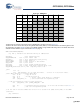
The return values for corresponding Table calls are tabulated as
shown in Table 9-11 on page 17
Table 9-11. Return values for Table Read
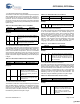
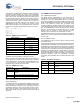
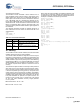
Table 9-8. ProtectBlock Parameters
Name Address Description
KEY1 0,F8h 3Ah
KEY2 0,F9h Stack Pointer value when SSC is
executed.
CLOCK 0,FCh Clock divider used to set the write pulse
width.
DELAY 0,FEh For a CPU speed of 12 MHz set to 56h.
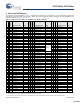
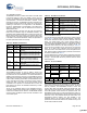
Table 9-9. EraseAll Parameters
Name Address Description
KEY1 0,F8h 3Ah
KEY2 0,F9h Stack Pointer value when SSC is
executed.
CLOCK 0,FCh Clock divider used to set the write pulse
width.
DELAY 0,FEh For a CPU speed of 12 MHz set to 56h
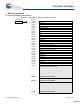
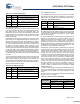
Table 9-10. Table Read Parameters
Name Address Description
KEY1 0,F8h 3Ah
KEY2 0,F9h Stack Pointer value when SSC is
executed.
BLOCKID 0,FAh Table number to read.
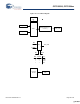
Table Number
Return Value
A X
0
Revision ID Family ID
1
Internal Revision Counter 0xFF
2-7
0xFF 0xFF
[+] Feedback [+] Feedback