
Full Speed USB Controller Specification Sheet


CY7C64215
Document 38-08036 Rev. *C Page 15 of 30
DC Electrical Characteristics
DC Chip-Level Specifications
The following table lists guaranteed maximum and minimum specifications for the voltage and temperature ranges: 4.75V to 5.25V
and 0°C <
T
A
< 70°C, or 3.0V to 3.6V and 0°C < T
A
< 70°C, respectively. Typical parameters apply to 5V and 3.3V at 25°C and are
for design guidance only.
DC General Purpose IO Specifications
The following table lists guaranteed maximum and minimum specifications for the voltage and temperature ranges: 4.75V to 5.25V
and 0°C <
T
A
< 70°C, or 3.0V to 3.6V and 0°C < T
A
< 70°C, respectively. Typical parameters apply to 5V and 3.3V at 25°C and are
for design guidance only.
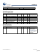
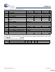
Table 8. DC Chip-Level Specifications
Parameter Description Min Typ Max Unit Notes
Vdd Supply Voltage 3.0 – 5.25 V See DC POR and LVD specifications, Table
16 on page 19. USB hardware is not
functional when Vdd is between 3.6V - 4.35V.
I
DD5
Supply Current, IMO = 24 MHz (5V) – 14 27 mA Conditions are Vdd = 5.0V, T
A
= 25°C, CPU
= 3 MHz, SYSCLK doubler disabled, VC1 =
1.5 MHz, VC2 = 93.75 kHz, VC3 = 93.75 kHz,
analog power = off.
I
DD3
Supply Current, IMO = 24 MHz (3.3V) – 8 14 mA Conditions are Vdd = 3.3V, T
A
= 25°C, CPU
= 3 MHz, SYSCLK doubler disabled, VC1 =
1.5 MHz, VC2 = 93.75 kHz, VC3 = 0.367 kHz,
analog power = off.
I
SB
Sleep (Mode) Current with POR, LVD, Sleep
Timer, and WDT.
[2]
– 3 6.5 μA Conditions are with internal slow speed oscil-
lator, Vdd = 3.3V, 0°C <
T
A
< 55°C, analog
power = off.
I
SBH
Sleep (Mode) Current with POR, LVD, Sleep
Timer, and WDT at high temperature.
[2]
– 4 25 μA Conditions are with internal slow speed oscil-
lator, Vdd = 3.3V, 55°C < T
A
< 70°C, analog
power = off.
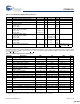
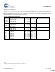
Table 9. DC GPIO Specifications
Parameter Description Min Typ Max Unit Notes
R
PU
Pull-Up Resistor 4 5.6 8 kΩ
R
PD
Pull-Down Resistor 4 5.6 8 kΩ
V
OH
High Output Level Vdd – 1.0 – – V IOH = 10 mA, Vdd = 4.75 to 5.25V (8 total loads, 4
on even port pins (for example, P0[2], P1[4]), 4 on
odd port pins (for example, P0[3], P1[5])). 80 mA
maximum combined IOH budget.
V
OL
Low Output Level – – 0.75 V IOL = 25 mA, Vdd = 4.75 to 5.25V (8 total loads, 4
on even port pins (for example, P0[2], P1[4]), 4 on
odd port pins (for example, P0[3], P1[5])). 150 mA
maximum combined IOL budget.
V
IL
Input Low Level – – 0.8 V Vdd = 3.0 to 5.25.
V
IH
Input High Level 2.1 – V Vdd = 3.0 to 5.25.
V
H
Input Hysteresis – 60 – mV
I
IL
Input Leakage (Absolute Value) – 1 – nA Gross tested to 1 μA.
C
IN
Capacitive Load on Pins as Input – 3.5 10 pF Package and pin dependent. Temp = 25°C.
C
OUT
Capacitive Load on Pins as Output – 3.5 10 pF Package and pin dependent. Temp = 25°C.
Note
2. Standby current includes all functions (POR, LVD, WDT, Sleep Time) needed for reliable system operation. This should be compared with devices that have similar
functions enabled.
[+] Feedback [+] Feedback