
Full Speed USB Controller Specification Sheet


CY7C64215
Document 38-08036 Rev. *C Page 16 of 30
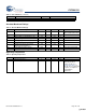
DC Full-Speed USB Specifications
The following table lists guaranteed maximum and minimum specifications for the voltage and temperature ranges: 4.75V to 5.25V
and 0°C <
T
A
< 70°C, or 3.0V to 3.6V and 0°C < T
A
< 70°C, respectively. Typical parameters apply to 5V and 3.3V at 25°C and are
for design guidance only.
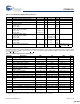
DC Analog Output Buffer Specifications
The following tables list guaranteed maximum and minimum specifications for the voltage and temperature ranges: 4.75V to 5.25V
and 0°C <
T
A
< 70°C, or 3.0V to 3.6V and 0°C < T
A
< 70°C, respectively. Typical parameters apply to 5V and 3.3V at 25°C and are
for design guidance only.
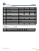
Table 10. DC Full-Speed (12 Mbps) USB Specifications
Parameter Description Min Typ Max Unit Notes
USB Interface
V
DI
Differential Input Sensitivity 0.2 – – V | (D+) – (D–) |
V
CM
Differential Input Common Mode Range 0.8 – 2.5 V
V
SE
Single Ended Receiver Threshold 0.8 – 2.0 V
C
IN
Transceiver Capacitance – – 20 pF
I
IO
High-Z State Data Line Leakage –10 – 10 μA0V < V
IN
< 3.3V.
R
EXT
External USB Series Resistor 23 – 25 Ω In series with each USB pin.
V
UOH
Static Output High, Driven 2.8 – 3.6 V 15 kΩ ± 5% to Ground. Internal pull-up
enabled.
V
UOHI
Static Output High, Idle 2.7 – 3.6 V 15 kΩ ± 5% to Ground. Internal pull-up
enabled.
V
UOL
Static Output Low – – 0.3 V 15 kΩ ± 5% to Ground. Internal pull-up
enabled.
Z
O
USB Driver Output Impedance 28 – 44 Ω Including R
EXT
Resistor.
V
CRS
D+/D– Crossover Voltage 1.3 – 2.0 V
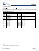
Table 11. 5V DC Analog Output Buffer Specifications
Parameter Description Min Typ Max Unit Notes
V
OSOB
Input Offset Voltage (Absolute Value) – 3 12 mV
TCV
OSOB
Average Input Offset Voltage Drift – +6 – μV/°C
V
CMOB
Common-Mode Input Voltage Range 0.5 – Vdd - 1.0 V
R
OUTOB
Output Resistance
Power = Low
Power = High
–
–
0.6
0.6
–
–
W
W
V
OHIGHOB
High Output Voltage Swing
(Load = 32 ohms to Vdd/2)
Power = Low
Power = High
0.5 x Vdd
+ 1.1
0.5 x Vdd
+ 1.1
–
–
–
–
V
V
V
OLOWOB
Low Output Voltage Swing
(Load = 32 ohms to Vdd/2)
Power = Low
Power = High
–
–
–
–
0.5 x Vdd
– 1.3
0.5 x Vdd
– 1.3
V
V
I
SOB
Supply Current Including Bias Cell (No Load)
Power = Low
Power = High
–
–
1.1
2.6
5.1
8.8
mA
mA
PSRR
OB
Supply Voltage Rejection Ratio 53 64 – dB (0.5 x Vdd – 1.3) <
V
OUT
< (Vdd – 2.3).
[+] Feedback [+] Feedback