
Full Speed USB Controller Specification Sheet


CY7C64215
Document 38-08036 Rev. *C Page 18 of 30
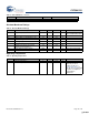
DC Analog enCoRe III Block Specifications
The following table lists guaranteed maximum and minimum specifications for the voltage and temperature ranges: 4.75V to 5.25V
and 0°C <
T
A
< 70°C, or 3.0V to 3.6V and 0°C < T
A
< 70°C, respectively. Typical parameters apply to 5V and 3.3V at 25°C and are
for design guidance only.
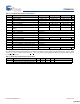
Table 14. 3.3V DC Analog Reference Specifications
Parameter Description Min Typ Max Unit
BG Bandgap Voltage Reference 1.28 1.30 1.32 V
– AGND = Vdd/2
[3]
Vdd/2 – 0.03 Vdd/2 – 0.01 Vdd/2 + 0.005 V
– AGND = 2 x BandGap
[3]
Not Allowed
– AGND = P2[4] (P2[4] = Vdd/2) P2[4] – 0.008 P2[4] + 0.001 P2[4] + 0.009 V
– AGND = BandGap
[3]
BG – 0.009 BG + 0.005 BG + 0.015 V
– AGND = 1.6 x BandGap
[3]
1.6 x BG – 0.027 1.6 x BG – 0.010 1.6 x BG + 0.018 V
– AGND Column to Column Variation (AGND =
Vdd/2)
[3]
–0.034 0.000 0.034 V
– RefHi = Vdd/2 + BandGap Not Allowed
– RefHi = 3 x BandGap Not Allowed
– RefHi = 2 x BandGap + P2[6] (P2[6] = 0.5V) Not Allowed
– RefHi = P2[4] + BandGap (P2[4] = Vdd/2) Not Allowed
– RefHi = P2[4] + P2[6] (P2[4] = Vdd/2, P2[6] = 0.5V) P2[4] + P2[6] – 0.075 P2[4] + P2[6] – 0.009 P2[4] + P2[6] + 0.057 V
– RefHi = 3.2 x BandGap Not Allowed
– RefLo = Vdd/2 – BandGap Not Allowed
– RefLo = BandGap Not Allowed
– RefLo = 2 x BandGap - P2[6] (P2[6] = 0.5V) Not Allowed
– RefLo = P2[4] – BandGap (P2[4] = Vdd/2) Not Allowed
– RefLo = P2[4]-P2[6] (P2[4] = Vdd/2, P2[6] = 0.5V) P2[4] – P2[6] – 0.048 P2[4] – P2[6] + 0.022 P2[4] – P2[6] + 0.092 V
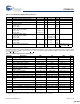
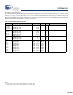
Table 15. DC Analog enCoRe III Block Specifications
Parameter Description Min Typ Max Unit Notes
R
CT
Resistor Unit Value (Continuous Time) – 12.2 – kΩ
C
SC
Capacitor Unit Value (Switched Capacitor) – 80 – fF
[+] Feedback [+] Feedback