
Full Speed USB Controller Specification Sheet

CY7C64215
Document 38-08036 Rev. *C Page 2 of 30
Applications
■
PC HID devices
❐
Mouse (Optomechanical, Optical, Trackball)
❐
Keyboards
❐
Joysticks
■
Gaming
❐
Game Pads
❐
Console Keyboards
■
General Purpose
❐
Barcode Scanners
❐
POS Terminal
❐
Consumer Electronics
❐
Toys
❐
Remote Controls
❐
USB to Serial
enCoRe III Functional Overview
The enCoRe III is based on flexible PSoC architecture and is a
full-featured, full-speed (12 Mbps) USB part. Configurable
analog, digital, and interconnect circuitry enable a high level of
integration in a host of consumer, and communication applica-
tions.
This architecture allows the user to create customized peripheral
configurations that match the requirements of each individual
application. Additionally, a fast CPU, Flash program memory,
SRAM data memory, and configurable IO are included in both
28-pin SSOP and 56-pin QFN packages.
The enCoRe III architecture, as illustrated in Figure , is
comprised of four main areas: enCoRe III Core, Digital System,
Analog System, and System Resources including a full-speed
USB port. Configurable global busing allows all the device
resources to combine into a complete custom system. The
enCoRe III CY7C64215 can have up to seven IO ports that
connect to the global digital and analog interconnects, providing
access to 4 digital blocks and 6 analog blocks.
enCoRe III Core
The enCoRe III Core is a powerful engine that supports a rich
feature set. The core includes a CPU, memory, clocks, and
configurable GPIO (General Purpose IO).
The M8C CPU core is a powerful processor with speeds up to 24
MHz, providing a four MIPS 8-bit Harvard architecture micropro-
cessor. The CPU utilizes an interrupt controller with up to 20
vectors, to simplify programming of real-time embedded events.
Program execution is timed and protected using the included
Sleep and Watch Dog Timers (WDT).
Memory encompasses 16K of Flash for program storage, 1K of
SRAM for data storage, and up to 2K of EEPROM emulated
using the Flash. Program Flash utilizes four protection levels on
blocks of 64 bytes, allowing customized software IP protection.
enCoRe III incorporates flexible internal clock generators,
including a 24 MHz IMO (internal main oscillator) accurate to 8%
over temperature and voltage. The 24 MHz IMO is doubled to 48
MHz for use by the digital system, if needed. The 48 MHz clock
is required to clock the USB block and must be enabled for USB
communication. A low power 32 kHz ILO (internal low speed
oscillator) is provided for the Sleep timer and WDT. The clocks,
together with programmable clock dividers (as a System
Resource), provide the flexibility to integrate almost any timing
requirement into the enCoRe III. In USB systems, the IMO
self-tunes to ±0.25% accuracy for USB communication.
enCoRe III GPIOs provide connection to the CPU, digital and
analog resources of the device. Each pin’s drive mode may be
selected from eight options, allowing great flexibility in external
interfacing. Every pin also has the capability to generate a
system interrupt on high level, low level, and change from last
read.
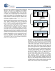
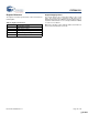
The Digital System
The Digital System is composed of four digital enCoRe III blocks.
Each block is an 8-bit resource that is used alone or combined
with other blocks to form 8, 16, 24, and 32-bit peripherals, which
are called user module references.
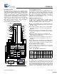
Figure 1. Digital System Block Diagram
Digital configurations that can be built from the blocks include
those listed below.
■
PWMs, Timers and Counters (8-bit and 16-bit)
■
UART 8-bit with selectable parity
■
SPI master and slave
■
I
2
C Master
■
RF Interface: Interface to Cypress CYFI Radio
The digital blocks is connected to any GPIO through a series of
global buses that can route any signal to any pin. The buses also
allow for signal multiplexing and for performing logic operations.
This configurability frees your designs from the constraints of a
fixed peripheral controller.
DIGITAL SYSTEM
To System Bus
D
i
g
i
t
a
l
C
l
o
c
k
s
F
r
o
m
C
o
r
e
Digital enCoRe III Block Array
To Analog
System
8
Row Input
Configuration
Row Out put
Configuration
88
8 Row 0
DBB00 DBB01 DCB02 DCB03
4
4
GIE[7:0]
GIO[7:0]
GOE[7:0]
GOO[7:0]
Global Digital
Interconnect
Port 1
Port 0
Port 3
Port 2
Port 5
Port 4
Port 7
[+] Feedback [+] Feedback