
Full Speed USB Controller Specification Sheet


CY7C64215
Document 38-08036 Rev. *C Page 25 of 30
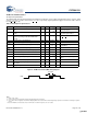
AC Programming Specifications
The following table lists guaranteed maximum and minimum specifications for the voltage and temperature ranges: 4.75V to 5.25V
and 0°C <
T
A
< 70°C, or 3.0V to 3.6V and 0°C < T
A
< 70°C, respectively. Typical parameters apply to 5V and 3.3V at 25°C and are
for design guidance only.
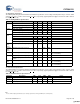
AC I
2
C Specifications
The following table lists guaranteed maximum and minimum specifications for the voltage and temperature ranges: 4.75V to 5.25V
and 0°C <
T
A
< 70°C, or 3.0V to 3.6V and 0°C < T
A
< 70°C, respectively. Typical parameters apply to 5V and 3.3V at 25°C and are
for design guidance only.
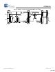
Table 25. AC Programming Specifications
Parameter Description Min Typ Max Unit Notes
T
RSCLK
Rise Time of SCLK 1 – 20 ns
T
FSCLK
Fall Time of SCLK 1 – 20 ns
T
SSCLK
Data Set up Time to Falling Edge of SCLK 40 – – ns
T
HSCLK
Data Hold Time from Falling Edge of SCLK 40 – – ns
F
SCLK
Frequency of SCLK 0 – 8 MHz
T
ERASEB
Flash Erase Time (Block) – 10 – ms
T
WRITE
Flash Block Write Time – 30 – ms
T
DSCLK
Data Out Delay from Falling Edge of SCLK – – 45 ns Vdd > 3.6
T
DSCLK3
Data Out Delay from Falling Edge of SCLK – – 50 ns 3.0 < Vdd < 3.6
Table 26. AC Characteristics of the I
2
C SDA and SCL Pins for Vdd
Parameter Description
Standard Mode Fast Mode
Unit Notes
Min Max Min Max
F
SCLI2C
SCL Clock Frequency 0 100 0 400 kHz
T
HDSTAI2C
Hold Time (repeated) START Condition. After
this period, the first clock pulse is generated.
4.0 –0.6– μs
T
LOWI2C
LOW Period of the SCL Clock 4.7 –1.3– μs
T
HIGHI2C
HIGH Period of the SCL Clock 4.0 –0.6– μs
T
SUSTAI2C
Setup Time for a Repeated START Condition 4.7 –0.6– μs
T
HDDATI2C
Data Hold Time 0 –0– μs
T
SUDATI2C
Data Setup Time 250 – 100
[12]
–ns
T
SUSTOI2C
Setup Time for STOP Condition 4.0 –0.6– μs
T
BUFI2C
Bus Free Time Between a STOP and START
Condition
4.7 –1.3– μs
T
SPI2C
Pulse Width of spikes are suppressed by the
input filter.
– – 0 50 ns
Note
12. A Fast-Mode I2C-bus device can be used in a Standard-Mode I2C-bus system, but the requirement tSU;DAT Š 250 ns must then be met. This automatically
be the case if the device does not stretch the LOW period of the SCL signal. If such device does stretch the LOW period of the SCL signal, it must output the
next data bit to the SDA line trmax + tSU;DAT = 1000 + 250 = 1250 ns (according to the Standard-Mode I2C-bus specification) before the SCL line is released.
[+] Feedback [+] Feedback