
Full Speed USB Controller Specification Sheet

CY7C64215
Document 38-08036 Rev. *C Page 3 of 30
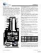
The Analog System
The Analog System is composed of six configurable blocks,
comprised of an opamp circuit allowing the creation of complex
analog signal flows. Analog peripherals are very flexible and are
customized to support specific application requirements.
enCoRe III analog function supports the Analog-to-digital
converters (with 6 to 14-bit resolution, selectable as Incremental,
and Delta Sigma) and programmable threshold comparator).
Analog blocks are arranged in two columns of three, with each
column comprising one CT (Continuous Time - AC B00 or AC
B01) and two SC (Switched Capacitor - ASC10 and ASD20 or
ASD11 and ASC21) blocks, as shown in Figure 2.
Figure 2. Analog System Block Diagram
The Analog Multiplexer System
The Analog Mux Bus can connect to every GPIO pin in ports 0–5.
Pins which are connected to the bus individually or in any combi-
nation. The bus also connects to the analog system for analysis
with comparators and analog-to-digital converters. It is split into
two sections for simultaneous dual-channel processing. An
additional 8:1 analog input multiplexer provides a second path to
bring Port 0 pins to the analog array.
Additional System Resources
System Resources provide additional capability useful to
complete systems. Additional resources include a multiplier,
decimator, low voltage detection, and power-on reset. Brief
statements describing the merits of each resource follow.
■
Full-Speed USB (12 Mbps) with five configurable endpoints and
256 bytes of RAM. No external components required except
two series resistors.
■
Two multiply accumulates (MACs) provide fast 8-bit multipliers
with 32-bit accumulate, to assist in both general math and
digital filters.
■
The decimator provides a custom hardware filter for digital
signal processing applications including the creation of Delta
Sigma ADCs.
■
Digital clock dividers provide three customizable clock
frequencies for use in applications. The clocks are routed to
both the digital and analog systems.
■
The I2C module provides 100 and 400 kHz communication over
two wires. Slave, master, and multi-master modes are all
supported.
■
Low Voltage Detection (LVD) interrupts can signal the appli-
cation of falling voltage levels, while the advanced POR (Power
On Reset) circuit eliminates the need for a system supervisor.
enCoRe III Device Characteristics
enCoRe III devices have four digital blocks and six analog
blocks. The following table lists the resources available for
specific enCoRe III device.
Getting Started
The quickest path to understanding enCoRe III silicon is by
reading this data sheet and using the PSoC Designer Integrated
Development Environment (IDE). This data sheet is an overview
of the enCoRe III integrated circuit and presents specific pin,
register, and electrical specifications. enCoRe III is based on the
architecture of the CY8C24794. For in-depth information, along
ACB00 ACB01
Block
Ar r a y
Array Input
Configuration
ACI1[1:0]
ASD20
ACI0[1:0]
P0[6]
P0[4]
P0[2]
P0[0]
P2[2]
P2[0]
P2[6]
P2[4]
RefIn
AGNDIn
P0[7]
P0[5]
P0[3]
P0[1]
P2[3]
P2[1]
Reference
Generators
AGNDIn
RefIn
Bandgap
RefHi
Ref Lo
AGND
ASD11
ASC21
ASC10
Interface to
Digital System
M8C Interface (Address Bus, Data Bus, Etc.)
Analog Refere nce
All IO
(Except Port 7)
Analog
Mux Bus
Table 1. enCoRe III Device Characteristics
Part
Number
Digital
IO
Digital
Rows
Digital
Blocks
Analog
Inputs
Analog
Outputs
Analog
Columns
Analog
Blocks
SRAM
Size
Flash
Size
CY7C64215
-28PVXC
up to
22
1 4 22 2 2 6 1K 16K
CY7C64215
-56LFXC
up to
50
1 4 48 2 2 6 1K 16K
[+] Feedback [+] Feedback