
Full Speed USB Controller Specification Sheet
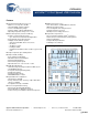

CY7C64215
Document 38-08036 Rev. *C Page 8 of 30
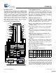
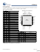
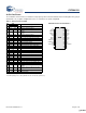
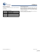
56-Pin Part Pinout
The CY7C64215 enCoRe III device is available in a 56-pin package which is listed and illustrated in the following table. Every port pin
(labeled “P”) is capable of Digital IO. However, Vss and Vdd are not capable of Digital IO.
Table 2. 56-Pin Part Pinout (MLF*)
Pin
No.
Type
Name Description
CY7C64215 56-Pin enCoRe III Device
Digital Analog
1 IO I, M P2[3] Direct switched capacitor block input.
2 IO I, M P2[1] Direct switched capacitor block input.
3 IO M P4[7]
4 IO M P4[5]
5 IO M P4[3]
6 IO M P4[1]
7 IO M P3[7]
8 IO M P3[5]
9 IO M P3[3]
10 IO M P3[1]
11 IO M P5[7]
12 IO M P5[5]
13 IO M P5[3]
14 IO M P5[1]
15 IO M P1[7] I2C Serial Clock (SCL).
16 IO M P1[5] I2C Serial Data (SDA).
17 IO M P1[3]
18 IO M P1[1] I2C Serial Clock (SCL), ISSP-SCLK.
19 Power Vss Ground connection.
20 USB D+
21 USB D-
22 Power Vdd Supply voltage.
23 IO P7[7]
24 IO P7[0]
25 IO M P1[0] I2C Serial Data (SDA), ISSP-SDATA.
26 IO M P1[2]
27 IO M P1[4]
28 IO M P1[6]
29 IO M P5[0]
Pin
No.
Type
Name Description30 IO M P5[2] Digital Analog
31 IO M P5[4] 44 IO M P2[6] External Voltage Reference (VREF) input.
32 IO M P5[6] 45 IO I, M P0[0] Analog column mux input.
33 IO M P3[0] 46 IO I, M P0[2] Analog column mux input and column output.
34 IO M P3[2] 47 IO I, M P0[4] Analog column mux input and column output.
35 IO M P3[4] 48 IO I, M P0[6] Analog column mux input.
36 IO M P3[6] 49 Power Vdd Supply voltage.
37 IO M P4[0] 50 Power Vss Ground connection.
38 IO M P4[2] 51 IO I, M P0[7] Analog column mux input.
39 IO M P4[4] 52 IO IO, M P0[5] Analog column mux input and column output
40 IO M P4[6] 53 IO IO, M P0[3] Analog column mux input and column output.
41 IO I, M P2[0] Direct switched capacitor block input. 54 IO I, M P0[1] Analog column mux input.
42 IO I, M P2[2] Direct switched capacitor block input. 55 IO M P2[7]
43 IO M P2[4] External Analog Ground (AGND) in-
put.
56 IO MP2[5]
LEGEND A = Analog, I = Input, O = Output, and M = Analog Mux Input.
* The MLF package has a center pad that must be connected to ground (Vss).
MLF
(Top View)
A, I, M, P2[3]
A, I, M, P2[1]
M, P4[7]
M, P4[5]
M, P4[3]
M, P4[1]
M, P3[7]
M, P3[5]
M, P3[3]
M, P3[1]
M, P5[7]
M, P5[5]
M, P5[3]
M, P5[1]
1
2
3
4
5
6
7
8
9
10
11
12
13
14
M, I2C SCL, P1[7]
M, I2C SDA, P1[5]
M, P1[3]
M, I2C SCL, P1[1]
Vss
D+
D-
Vdd
P7[7]
P7[0]
M, I2C SDA, P1[0]
M, P1[2]
M, P1[4]
M, P1[6]
15
16
17
18
19
20
21
22
23
24
25
26
27
28
P2[4], M
P2[6], M
P0[0], A, I, M
P0[2], A, I, M
P0[4], A, I, M
P0[6], A, I, M
Vdd
Vss
P0[7], A, I, M
P0[5], A, IO, M
P0[3], A, IO, M
P0[1], A, I, M
P2[7], M
P2[5], M
43
44
45
46
47
48
49
50
51
52
53
54
55
56
P2[2], A, I, M
P2[0], A, I, M
P4[6], M
P4[4], M
P4[2], M
P4[0], M
P3[6], M
P3[4], M
P3[2], M
P3[0], M
P5[6], M
P5[4], M
P5[2], M
P5[0], M
42
41
40
39
38
37
36
35
34
33
32
31
30
29
[+] Feedback [+] Feedback