
Full Speed USB Controller Specification Sheet

CY7C64215
Document 38-08036 Rev. *C Page 9 of 30
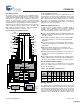
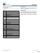
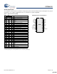
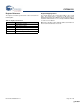
28-Pin Part Pinout
The CY7C64215 enCoRe III device is available in a 28-pin package which is listed and illustrated in the following table. Every port pin
(labeled with a “P”) is capable of Digital IO. However, Vss and Vdd are not capable of Digital IO.
Table 3. 28-Pin Part Pinout (SSOP)
Pin
No.
Type
Name Description
CY7C64215 28-Pin enCoRe III Device
Digital Analog
1 Power GND Ground connection
2 IO I, M P0[7] Analog column mux input.
3 IO IO,M P0[5] Analog column mux input and column
output
4 IO IO,M P0[3] Analog column mux input and column
output.
5 IO I,M P0[1] Analog column mux input.
6 IO M P2[5]
7 IO M P2[3] Direct switched capacitor block input.
8 IO M P2[1] Direct switched capacitor block input.
9 IO M P1[7] I2C Serial Clock (SCL).
10 IO M P1[5] I2C Serial Data (SDA).
11 IO M P1[3]
12 IO M P1[1] I2C Serial Clock (SCL), ISSP-SCLK.
13 Power GND Ground connection
14 USB D+
15 USB D-
16 Power Vdd Supply voltage.
17 IO M P1[0] I2C Serial Data (SDA), ISSP-SDATA.
18 IO M P1[2]
19 IO M P1[4]
20 IO M P1[6]
21 IO M P2[0] Direct switched capacitor block input.
22 IO M P2[2] Direct switched capacitor block input.
23 IO M P2[4] External Analog Ground (AGND) input.
24 IO M P0[0] Analog column mux input.
25 IO M P0[2] Analog column mux input and column
output.
26 IO M P0[4] Analog column mux input and column
output.
27 IO M P0[6] Analog column mux input.
28 Power Vdd Supply voltage.
LEGEND A = Analog, I = Input, O = Output, and M = Analog Mux Input.
* The MLF package has a center pad that must be connected to ground (Vss).
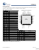
SSOP
1
2
3
4
5
6
7
8
9
10
11
12
13
14
28
27
26
25
24
23
22
21
20
19
18
17
16
15
Vdd
P0[6], AI
P0[4], AI
P0[2], AI
P0[0], AI
P2[4]
P2[2], AI
P2[0], AI
P1[6]
P1[4]
P1[2]
P1[0], I2C SDA
Vdd
D-
Vss
AI, P0[7]
AIO, P0 [5 ]
AIO, P0 [3 ]
AI, P0[1]
P2[5]
AI, P2[3]
AI, P2[1]
I2C SCL, P1[7]
I2C SD A, P1[5 ]
P1[3]
I2 C SC L, P1 [1 ]
Vss
D+
[+] Feedback [+] Feedback