
PCB Design Recommendations Specification Sheet

November 21, 2002 Document No. 001-43117 Rev. ** 1
EZ-USB FX2™ PCB
Design Recommendations
Introduction
This application note presents recommendations for design-
ing with the Cypress Semiconductor EZ-USB FX2™ compo-
nent. Techniques for high-speed design should be applied to
circuits using the EZ-USB FX2. Due to the packaging and
high performance characteristics of the EZ-USB FX2, consid-
eration of the PCB thermal design is required.
CY4611 EZ-USB FX2 USB to ATA Reference
Design
A complete design using the Cypress CY7C68013 EZ-USB
FX2 is available. The design implements the recommenda-
tions of this application note. It may be useful for the reader to
download the CY4611 Reference Design Files from the
Cypress Support page for Reference Designs.
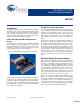
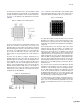
Figure 1. FX2 (CY4611) USB to ATA Reference Design
Cypress offers the CY4611 EZ-USB FX2 USB to ATA Refer-
ence Design as an evaluation platform for developers wishing
to integrate a USB 2.0 Peripheral Controller into their applica-
tion. The kit includes the EZ-USB FX2 USB to ATA evaluation
board, USB cable, schematics, bill of material, PCB Gerber
files, and other documentation.
EZ-USB FX2 Package Description
The CY7C68013-56LFC EZ-USB FX2 component is pack-
aged as a 56-pad, 8-mm by 8-mm, 1-mm high, QFN (Quad
Flatpack No leads) package. Please refer to the latest
CY7C68013 EZ-USB FX2 USB Microcontroller High-speed
USB Peripheral Controller data sheet for the detailed pack-
age drawing. The data sheet is Cypress specification 38-
08012.
This package is comparable to the Amkor MicroLeadFrame™
package. It is a plastic encapsulated, near-chip scale pack-
age using solder lands instead of leads or balls. It uses a cop-
per leadframe substrate that provides for short die to frame
lead length giving good high-frequency performance. It has
an exposed die paddle that enables good thermal transfer out
of the package. For further details about this package and
methods and processes associated with its assembly to a
printed circuit board, please refer to the manufacturer's appli-
cation note identified in the References section of this docu-
ment.
Electrical Design Recommendations
USB 2.0 high-speed signaling is used to transfer data at 480
Mbps. This rate is 40 times higher than the highest speed of
the USB 1.1 specification, full-speed signaling that operates
at a 12-Mbps rate. High-speed signaling requires a greater
level of attention to electrical design than previously required
for USB designs. Careful attention to component selection,
supply decoupling, signal line impedance, and noise are
required when designing for high-speed USB. These physical
issues are mostly effected by the PCB design and is pre-
sented in the PCB Design Recommendation section.
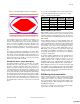
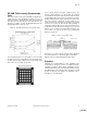
One key measurement of USB data signal quality is the eye
pattern. The eye pattern is a representation of USB signaling
that provides minimum and maximum voltage levels as well
as signal jitter. Section 7.1 in the USB 2.0 Specification pro-
vides detailed explanation and requirements for a compliant
eye pattern. Figure 2 is an eye diagram of high-speed signal-
ing as measured on the EZ-USB FX2 component.
AN1196
[+] Feedback [+] Feedback