
Synchronous Dual-Port RAM Specification Sheet

FLEx18™ 3.3V 64K/128K x 36 and
128K/256K x 18 Synchronous Dual-Port RAM
CY7C0837AV, CY7C0830AV
CY7C0831AV, CY7C0832AV
CY7C0832BV, CY7C0833AV
Cypress Semiconductor Corporation • 198 Champion Court • San Jose
,
CA 95134-1709 • 408-943-2600
Document #: 38-06059 Rev. *S Revised March 03, 2009
Features
■
True Dual-Ported Memory Cells that Allow Simultaneous
Access of the Same Memory Location
■
Synchronous Pipelined Operation
■
Family of 512 Kbit, 1 Mbit, 2 Mbit, 4 Mbit, and 9 Mbit Devices
■
Pipelined Output Mode Allows Fast Operation
■
0.18 micron CMOS for Optimum Speed and Power
■
High Speed Clock to Data Access
■
3.3V Low Power
❐
Active as Low as 225 mA (typ)
❐
Standby as Low as 55 mA (typ)
■
Mailbox Function for Message Passing
■
Global Master Reset
■
Separate Byte Enables on Both Ports
■
Commercial and Industrial Temperature Ranges
■
IEEE 1149.1 Compatible JTAG Boundary Scan
■
144-Ball FBGA (13 mm × 13 mm) (1.0 mm pitch)
■
120 TQFP (14 mm x 14 mm x 1.4 mm)
■
Pb-Free Packages Available
■
Counter Wrap Around Control
❐
Internal Mask Register Controls Counter Wrap Around
❐
Counter-Interrupt Flags to Indicate Wrap Around
❐
Memory Block Retransmit Operation
■
Counter Readback on Address Lines
■
Mask Register Readback on Address Lines
■
Dual Chip Enables on Both Ports for Easy Depth Expansion
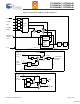
Functional Description
The FLEx18™ family includes 512 Kbit, 1 Mbit, 2 Mbit, 4 Mbit,
and 9 Mbit pipelined, synchronous, true dual port static RAMs
that are high speed, low power 3.3V CMOS. Two ports are
provided, permitting independent, simultaneous access to any
location in memory. The result of writing to the same location by
more than one port at the same time is undefined. Registers on
control, address, and data lines allow for minimal setup and hold
time.
During a Read operation, data is registered for decreased cycle
time. Each port contains a burst counter on the input address
register. After externally loading the counter with the initial
address, the counter increments the address internally (more
details to follow). The internal Write pulse width is independent
of the duration of the R/W
input signal. The internal Write pulse
is self-timed to allow the shortest possible cycle times.
A HIGH on CE0
or LOW on CE1 for one clock cycle powers down
the internal circuitry to reduce the static power consumption. One
cycle with chip enables asserted is required to reactivate the
outputs.
Additional features include: readback of burst-counter internal
address value on address lines, counter-mask registers to
control the counter wrap around, counter interrupt (CNTINT
)
flags, readback of mask register value on address lines,
retransmit functionality, interrupt flags for message passing,
JTAG for boundary scan, and asynchronous Master Reset
(MRST
).
The CY7C0833AV device in this family has limited features. See
Address Counter and Mask Register Operations
[16]
on page 6
for details.
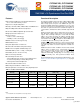
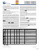
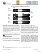
Table 1. Product Selection Guide
Density
512 Kbit
(32K x 18)
1 Mbit
(64K x 18)
2 Mbit
(128K x 18)
4 Mbit
(256K x 18)
9 Mbit
(512K x 18)
Part Number CY7C0837AV CY7C0830AV CY7C0831AV CY7C0832AV CY7C0832BV
[1]
CY7C0833AV
Maximum Speed (MHz) 167 167 167 167 133 133
Maximum Access Time -
Clock to Data (ns)
4.0 4.0 4.0 4.0 4.4 4.7
Typical Operating
Current (mA)
225 225 225 225 225 270
Package 144 FBGA 120 TQFP
144 FBGA
120 TQFP
144 FBGA
120 TQFP
144 FBGA
120 TQFP 144 FBGA
Note
1. CY7C0832AV and CY7C0832BV are functionally identical.
[+] Feedback