
Independent Clock Serializer and Reclocking Deserializer Specification Sheet

Independent Clock HOTLink II™ Serializer and
Reclocking Deserialize
r
CYV15G0104TRB
Cypress Semiconductor Corporation • 3901 North First Street • San Jose, CA 95134 • 408-943-2600
Document #: 38-02100 Rev. *B Revised July 8, 2005
Features
• Second-generation HOTLink
®
technology
• Compliant to SMPTE 292M and SMPTE 259M video
standards
• Single channel video serializer plus single channel
video reclocking deserializer
— 195- to 1500-Mbps serial data signaling rate
— Simultaneous operation at different signaling rates
• Supports reception of either 1.485 or 1.485/1.001 Gbps
data rate with the same training clock
• Internal phase-locked loops (PLLs) with no external
PLL components
• Supports half-rate and full-rate clocking
• Selectable differential PECL-compatible serial inputs
— Internal DC-restoration
• Redundant differential PECL-compatible serial outputs
— No external bias resistors required
— Internal source termination
— Signaling-rate controlled edge-rates
• Synchronous LVTTL parallel interface
• JTAG boundary scan
• Built-In Self-Test (BIST) for at-speed link testing
• Link Quality Indicator
— Analog signal detect
— Digital signal detect
• Low-power 1.8W @ 3.3V typical
• Single 3.3V supply
• Thermally enhanced BGA
• Pb-Free package option available
•0.25µ BiCMOS technology
Functional Description
The CYV15G0104TRB Independent Clock HOTLink II™
Serializer and Reclocking Deserializer is a point-to-point or
point-to-multipoint communications building block enabling
transfer of data over a variety of high-speed serial links
including SMPTE 292M and SMPTE 259M video applications.
It supports signaling rates in the range of 195 to 1500 Mbps
per serial link. The transmit and receive channels are
independent and can operate simultaneously at different
rates. The transmit channel accepts 10-bit parallel characters
in an Input Register and converts them to serial data. The
receive channel accepts serial data and converts it to 10-bit
parallel characters and presents these characters to an Output
Register. The received serial data can also be reclocked and
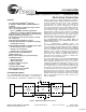
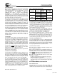
retransmitted through the reclocker serial outputs. Figure 1
illustrates typical connections between independent video co-
processors and corresponding CYV15G0104TRB chips.
The CYV15G0104TRB satisfies the SMPTE 259M and
SMPTE 292M compliance as per SMPTE EG34-1999 Patho-
logical Test Requirements.
As a second-generation HOTLink device, the
CYV15G0104TRB extends the HOTLink family with enhanced
levels of integration and faster data rates, while maintaining
serial-link compatibility (data and BIST) with other HOTLink
devices. The transmit (TX) channel of the CYV15G0104TRB
HOTLink II device accepts scrambled 10-bit transmission
characters. These characters are serialized and output from
dual Positive ECL (PECL) compatible differential trans-
mission-line drivers at a bit-rate of either 10- or 20-times the
input reference clock for that channel.
The receive (RX) channel of the CYV15G0104TRB HOTLink
II device accepts a serial bit-stream from one of two selectable
PECL-compatible differential line receivers, and using a
completely integrated Clock and Data Recovery PLL, recovers
the timing information necessary for data reconstruction. The
recovered bit-stream is reclocked and retransmitted through
the reclocker serial outputs. Also, the recovered serial data is
deserialized and presented to the destination host system.
The transmit and receive channels contain an independent
BIST pattern generator and checker, respectively. This BIST
hardware allows at-speed testing of the high-speed serial data
paths in each transmit and receive section, and across the
interconnecting links.
Figure 1. HOTLink II™ System Connections
Video Coprocessor
10
10
Video Coprocessor
10
10
Serial
Links
Independent
CYV15G0104TRB
Independent
Device
Device
Channel
CYV15G0104TRB
Channel
Reclocked
Output
Reclocked
Output
[+] Feedback