
Flow-Through SRAM Specification Sheet

CY7C1355C
CY7C1357C
Document #: 38-05539 Rev. *E Page 8 of 28
Functional Overview
The CY7C1355C/CY7C1357C is a synchronous flow-through
burst SRAM designed specifically to eliminate wait states
during Write-Read transitions. All synchronous inputs pass
through input registers controlled by the rising edge of the
clock. The clock signal is qualified with the Clock Enable input
signal (CEN
). If CEN is HIGH, the clock signal is not recog-
nized and all internal states are maintained. All synchronous
operations are qualified with CEN
. Maximum access delay
from the clock rise (t
CDV
) is 6.5 ns (133-MHz device).
Accesses can be initiated by asserting all three Chip Enables
(CE
1
, CE
2
, CE
3
) active at the rising edge of the clock. If Clock
Enable (CEN
) is active LOW and ADV/LD is asserted LOW,
the address presented to the device will be latched. The
access can either be a Read or Write operation, depending on
the status of the Write Enable (WE
). BW
X
can be used to
conduct Byte Write operations.
Write operations are qualified by the Write Enable (WE
). All
writes are simplified with on-chip synchronous self-timed Write
circuitry.
Three synchronous Chip Enables (CE
1
, CE
2
, CE
3
) and an
asynchronous Output Enable (OE
) simplify depth expansion.
All operations (Reads, Writes, and Deselects) are pipelined.
ADV/LD
should be driven LOW once the device has been
deselected in order to load a new address for the next
operation.
Single Read Accesses
A read access is initiated when the following conditions are
satisfied at clock rise: (1) CEN
is asserted LOW, (2) CE
1
, CE
2
,
and CE
3
are ALL asserted active, (3) the Write Enable input
signal WE
is deasserted HIGH, and 4) ADV/LD is asserted
LOW. The address presented to the address inputs is latched
into the address register and presented to the memory array
and control logic. The control logic determines that a read
access is in progress and allows the requested data to
propagate to the output buffers. The data is available within 7.5
ns (133-MHz device) provided OE
is active LOW. After the first
clock of the read access, the output buffers are controlled by
OE and the internal control logic. OE must be driven LOW in
order for the device to drive out the requested data. On the
subsequent clock, another operation (Read/Write/Deselect)
can be initiated. When the SRAM is deselected at clock rise
by one of the chip enable signals, its output will be tri-stated
immediately.
Burst Read Accesses
The CY7C1355C/CY7C1357C has an on-chip burst counter
that allows the user the ability to supply a single address and
conduct up to four Reads without reasserting the address
inputs. ADV/LD
must be driven LOW in order to load a new
address into the SRAM, as described in the Single Read
Access section above. The sequence of the burst counter is
determined by the MODE input signal. A LOW input on MODE
selects a linear burst mode, a HIGH selects an interleaved
burst sequence. Both burst counters use A0 and A1 in the
burst sequence, and will wrap around when incremented suffi-
ciently. A HIGH input on ADV/LD
will increment the internal
burst counter regardless of the state of chip enable inputs or
WE. WE is latched at the beginning of a burst cycle. Therefore,
the type of access (Read or Write) is maintained throughout
the burst sequence.
Single Write Accesses
Write access are initiated when the following conditions are
satisfied at clock rise: (1) CEN
is asserted LOW, (2) CE
1
, CE
2
,
and CE
3
are ALL asserted active, and (3) the Write signal WE
is asserted LOW. The address presented to the address bus
is loaded into the address register. The write signals are
latched into the Control Logic block. The data lines are
automatically tri-stated regardless of the state of the OE
input
signal. This allows the external logic to present the data on
DQs and DQP
X
.
On the next clock rise the data presented to DQs and DQP
X
(or a subset for byte write operations, see Truth Table for
details) inputs is latched into the device and the write is
complete. Additional accesses (Read/Write/Deselect) can be
initiated on this cycle.
The data written during the Write operation is controlled by
BW
X
signals. The CY7C1355C/CY7C1357C provides byte
write capability that is described in the Truth Table. Asserting
the Write Enable input (WE) with the selected Byte Write
Select input will selectively write to only the desired bytes.
Bytes not selected during a byte write operation will remain
unaltered. A synchronous self-timed Write mechanism has
been provided to simplify the Write operations. Byte Write
capability has been included in order to greatly simplify
Read/Modify/Write sequences, which can be reduced to
simple Byte Write operations.
Because the CY7C1355C/CY7C1357C is a common I/O
device, data should not be driven into the device while the
outputs are active. The Output Enable (OE
) can be deasserted
HIGH before presenting data to the DQs and DQP
X
inputs.
Doing so will tri-state the output drivers. As a safety
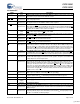
TMS JTAG serial input
Synchronous
Serial data-In to the JTAG circuit. Sampled on the rising edge of TCK. If the JTAG feature
is not being utilized, this pin can be disconnected or connected to V
DD
. This pin is not
available on TQFP packages.
TCK JTAG
Clock
Clock input to the JTAG circuitry. If the JTAG feature is not being utilized, this pin must
be connected to V
SS
. This pin is not available on TQFP packages.
NC – No Connects. Not internally connected to the die. 18 Mbit, 36 Mbit, 72 Mbit, 144 Mbit, 288
Mbit, 576 Mbit and 1G are address expansion pins and are not internally connected to the
die.
V
SS
/DNU Ground/DNU This pin can be connected to Ground or should be left floating.
Pin Definitions (continued)
Name I/O Description
[+] Feedback