
Flow-Through SRAM Specification Sheet

18-Mbit (512K x 36/1M x 18)
Flow-Through SRAM with NoBL™ Architecture
CY7C1371D
CY7C1373D
Cypress Semiconductor Corporation • 198 Champion Court • San Jose, CA 95134-1709 • 408-943-2600
Document #: 38-05556 Rev. *F Revised July 09, 2007
Features
• No Bus Latency™ (NoBL™) architecture eliminates dead
cycles between write and read cycles
• Supports up to 133-MHz bus operations with zero wait
states
— Data is transferred on every clock
• Pin-compatible and functionally equivalent to ZBT™
devices
• Internally self-timed output buffer control to eliminate the
need to use OE
• Registered inputs for flow through operation
• Byte Write capability
• 3.3V/2.5V IO power supply (V
DDQ
)
• Fast clock-to-output times
— 6.5 ns (for 133-MHz device)
• Clock Enable (CEN
) pin to enable clock and suspend
operation
• Synchronous self-timed writes
• Asynchronous Output Enable
• Available in JEDEC-standard Pb-free 100-pin TQFP,
Pb-free and non-Pb-free 119-Ball BGA and 165-Ball FBGA
package.
• Three chip enables for simple depth expansion
• Automatic Power down feature available using ZZ mode or
CE deselect
• IEEE 1149.1 JTAG-Compatible Boundary Scan
• Burst Capability — linear or interleaved burst order
• Low standby power
Functional Description
[1]
The CY7C1371D/CY7C1373D is a 3.3V, 512K x 36/1M x 18
Synchronous flow through Burst SRAM designed specifically
to support unlimited true back-to-back Read/Write operations
with no wait state insertion. The CY7C1371D/CY7C1373D is
equipped with the advanced No Bus Latency (NoBL) logic
required to enable consecutive Read/Write operations with
data being transferred on every clock cycle. This feature
dramatically improves the throughput of data through the
SRAM, especially in systems that require frequent Write-Read
transitions.
All synchronous inputs pass through input registers controlled
by the rising edge of the clock. The clock input is qualified by
the Clock Enable (CEN
) signal, which when deasserted
suspends operation and extends the previous clock cycle.
Maximum access delay from the clock rise is 6.5 ns (133-MHz
device).
Write operations are controlled by the two or four Byte Write
Select (BW
X
) and a Write Enable (WE) input. All writes are
conducted with on-chip synchronous self-timed write circuitry.
Three synchronous Chip Enables (CE
1
, CE
2
, CE
3
) and an
asynchronous Output Enable (OE
) provide for easy bank
selection and output tri-state control. To avoid bus contention,
the output drivers are synchronously tri-stated during the data
portion of a write sequence.
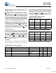
Selection Guide
133 MHz 100 MHz Unit
Maximum Access Time 6.5 8.5 ns
Maximum Operating Current 210 175 mA
Maximum CMOS Standby Current 70 70 mA
Note:
1. For best-practices recommendations, please refer to the Cypress application note System Design Guidelines on www.cypress.com.
[+] Feedback