CY7C68013A, CY7C68014A CY7C68015A, CY7C68016A EZ-USB FX2LP™ USB Microcontroller High-Speed USB Peripheral Controller 1. Features (CY7C68013A/14A/15A/16A) ■ USB 2.0 USB IF high-speed certified (TID # 40460272) ■ Single chip integrated USB 2.
CY7C68013A, CY7C68014A CY7C68015A, CY7C68016A Logic Block Diagram High performance micro using standard tools with lower-power options 24 MHz Ext. XTAL /0.5 /1.0 /2.0 I2C 8051 Core 12/24/48 MHz, four clocks/cycle Address (16) / Data Bus (8) x20 PLL VCC Data (8) Address (16) FX2LP 1.5k connected for full-speed D+ D– USB 2.0 XCVR Integrated full-speed and high-speed XCVR CY Smart USB 1.1/2.
CY7C68013A, CY7C68014A CY7C68015A, CY7C68016A 2. Applications frequency is 12 MHz. The clock frequency of the 8051 can be changed by the 8051 through the CPUCS register, dynamically.
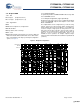
CY7C68013A, CY7C68014A CY7C68015A, CY7C68016A Table 1. Special Function Registers x 0 1 8x IOA SP 9x IOB EXIF Ax IOC INT2CLR Bx IOD IOE 2 3 4 5 6 7 8 9 A B C D E F DPL0 DPH0 DPL1 DPH1 DPS PCON TCON TMOD TL0 TL1 TH0 TH1 CKCON MPAGE INT4CLR OEA OEB OEC OED OEE SCON0 SBUF0 AUTOPTRH1 AUTOPTRL1 reserved AUTOPTRH2 AUTOPTRL2 reserved IE EP2468STAT EP24FIFOFLGS EP68FIFOFLGS AUTOPTRSET-UP 3.
CY7C68013A, CY7C68014A CY7C68015A, CY7C68016A The FX2LP jump instruction is encoded as follows: Table 3.
CY7C68013A, CY7C68014A CY7C68015A, CY7C68016A Table 4.
CY7C68013A, CY7C68014A CY7C68015A, CY7C68016A Figure 2. Reset Timing Plots RESET# RESET# VIL VIL 3.3V 3.0V 3.3V VCC VCC 0V 0V TRESET TRESET Power on Reset Powered Reset Table 5. Reset Timing Values 3.10 Program/Data RAM Condition TRESET Power on Reset with Crystal 5 ms Power on Reset with External Clock 200 μs + Clock stability time Powered Reset 200 μs 3.10.
CY7C68013A, CY7C68014A CY7C68015A, CY7C68016A Figure 3. Internal Code Memory, EA = 0 Inside FX2LP Outside FX2LP FFFF 7.5 KBytes USB regs and 4K FIFO buffers (RD#,WR#) E200 E1FF 0.
CY7C68013A, CY7C68014A CY7C68015A, CY7C68016A Figure 4. External Code Memory, EA = 1 Inside FX2LP Outside FX2LP FFFF 7.5 KBytes USB regs and 4K FIFO buffers (RD#,WR#) E200 E1FF 0.
CY7C68013A, CY7C68014A CY7C68015A, CY7C68016A 3.12 Endpoint RAM 3.12.3 Setup Data Buffer 3.12.1 Size A separate 8 byte buffer at 0xE6B8-0xE6BF holds the setup data from a CONTROL transfer. ■ 3× 64 bytes (Endpoints 0 and 1) ■ 8 × 512 bytes (Endpoints 2, 4, 6, 8) 3.12.4 Endpoint Configurations (High -speed Mode) Endpoints 0 and 1 are the same for every configuration. Endpoint 0 is the only CONTROL endpoint, and endpoint 1 can be either BULK or INTERRUPT. 3.12.
CY7C68013A, CY7C68014A CY7C68015A, CY7C68016A 3.12.5 Default Full-Speed Alternate Settings Table 6. Default Full-Speed Alternate Settings[4, 5] Alternate Setting 0 1 2 3 ep0 64 64 64 64 ep1out 0 64 bulk 64 int 64 int ep1in 0 64 bulk 64 int 64 int ep2 0 64 bulk out (2×) 64 int out (2×) 64 iso out (2×) ep4 0 64 bulk out (2×) 64 bulk out (2×) 64 bulk out (2×) ep6 0 64 bulk in (2×) 64 int in (2×) 64 iso in (2×) ep8 0 64 bulk in (2×) 64 bulk in (2×) 64 bulk in (2×) 3.12.
CY7C68013A, CY7C68014A CY7C68015A, CY7C68016A 3.13.3 GPIF and FIFO Clock Rates 3.15 ECC Generation[7] An 8051 register bit selects one of two frequencies for the internally supplied interface clock: 30 MHz and 48 MHz. Alternatively, an externally supplied clock of 5 MHz–48 MHz feeding the IFCLK pin can be used as the interface clock. IFCLK can be configured to function as an output clock when the GPIF and FIFOs are internally clocked.
CY7C68013A, CY7C68014A CY7C68015A, CY7C68016A 3.18 I2C Controller 3.18.2 I2C Interface Boot Load Access FX2LP has one I2C port that is driven by two internal controllers, one that automatically operates at boot time to load VID/PID/DID and configuration information, and another that the 8051 uses when running to control external I2C devices. The I2C port operates in master mode only.
CY7C68013A, CY7C68014A CY7C68015A, CY7C68016A 3.20 CY7C68013A/14A and CY7C68015A/16A Differences CY7C68013A is identical to CY7C68014A in form, fit, and functionality. CY7C68015A is identical to CY7C68016A in form, fit, and functionality. CY7C68014A and CY7C68016A have a lower suspend current than CY7C68013A and CY7C68015A respectively and are ideal for power sensitive battery applications. CY7C68015A and CY7C68016A are available in 56-pin QFN package only.
CY7C68013A, CY7C68014A CY7C68015A, CY7C68016A Figure 6.
CY7C68013A, CY7C68014A CY7C68015A, CY7C68016A Figure 7.
CY7C68013A, CY7C68014A CY7C68015A, CY7C68016A Figure 8.
CY7C68013A, CY7C68014A CY7C68015A, CY7C68016A Figure 9.
CY7C68013A, CY7C68014A CY7C68015A, CY7C68016A Figure 10.
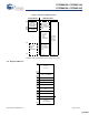
CY7C68013A, CY7C68014A CY7C68015A, CY7C68016A Figure 11. CY7C68013A 56-pin VFBGA Pin Assignment - Top View 1 2 3 4 5 6 7 8 A 1A 2A 3A 4A 5A 6A 7A 8A B 1B 2B 3B 4B 5B 6B 7B 8B C 1C 2C 3C 4C 5C 6C 7C 8C D 1D 2D 7D 8D E 1E 2E 7E 8E F 1F 2F 3F 4F 5F 6F 7F 8F G 1G 2G 3G 4G 5G 6G 7G 8G H 1H 2H 3H 4H 5H 6H 7H 8H Document #: 38-08032 Rev.
CY7C68013A, CY7C68014A CY7C68015A, CY7C68016A 4.1 CY7C68013A/15A Pin Descriptions The FX2LP Pin Descriptions follows.[10] Table 11. FX2LP Pin Descriptions 128 100 56 56 56 VFTQFP TQFP SSOP QFN BGA Name Type Default Description 10 9 10 3 2D AVCC Power N/A Analog VCC. Connect this pin to 3.3V power source. This signal provides power to the analog section of the chip. 17 16 14 7 1D AVCC Power N/A Analog VCC. Connect this pin to 3.3V power source.
CY7C68013A, CY7C68014A CY7C68015A, CY7C68016A Table 11. FX2LP Pin Descriptions (continued) 128 100 56 56 56 VFTQFP TQFP SSOP QFN BGA 34 28 99 77 Name Type Default Description Output L Breakpoint. This pin goes active (HIGH) when the 8051 address bus matches the BPADDRH/L registers and breakpoints are enabled in the BREAKPT register (BPEN = 1). If the BPPULSE bit in the BREAKPT register is HIGH, this signal pulses HIGH for eight 12-/24-/48-MHz clocks.
CY7C68013A, CY7C68014A CY7C68015A, CY7C68016A Table 11. FX2LP Pin Descriptions (continued) 128 100 56 56 56 VFTQFP TQFP SSOP QFN BGA Name Type Default Description 85 70 43 36 7F PA3 or WU2 IO/Z I Multiplexed pin whose function is selected by: (PA3) WAKEUP.7 and OEA.3 PA3 is a bidirectional IO port pin. WU2 is an alternate source for USB Wakeup, enabled by WU2EN bit (WAKEUP.1) and polarity set by WU2POL (WAKEUP.4).
CY7C68013A, CY7C68014A CY7C68015A, CY7C68016A Table 11. FX2LP Pin Descriptions (continued) 128 100 56 56 56 VFTQFP TQFP SSOP QFN BGA Name Type Default Description 55 45 30 23 5G PB5 or FD[5] IO/Z I Multiplexed pin whose function is selected by the (PB5) following bits: IFCONFIG[1..0]. PB5 is a bidirectional IO port pin. FD[5] is the bidirectional FIFO/GPIF data bus. 56 46 31 24 5F PB6 or FD[6] IO/Z I Multiplexed pin whose function is selected by the (PB6) following bits: IFCONFIG[1..0].
CY7C68013A, CY7C68014A CY7C68015A, CY7C68016A Table 11. FX2LP Pin Descriptions (continued) 128 100 56 56 56 VFTQFP TQFP SSOP QFN BGA Name Type Default Description 104 82 54 47 6B PD2 or FD[10] IO/Z I Multiplexed pin whose function is selected by the (PD2) IFCONFIG[1..0] and EPxFIFOCFG.0 (wordwide) bits. FD[10] is the bidirectional FIFO/GPIF data bus. 105 83 55 48 6A PD3 or FD[11] IO/Z I Multiplexed pin whose function is selected by the (PD3) IFCONFIG[1..0] and EPxFIFOCFG.
CY7C68013A, CY7C68014A CY7C68015A, CY7C68016A Table 11. FX2LP Pin Descriptions (continued) 128 100 56 56 56 VFTQFP TQFP SSOP QFN BGA Name Type Default Description 112 90 PE4 or RXD1OUT IO/Z I Multiplexed pin whose function is selected by the (PE4) PORTECFG.4 bit. PE4 is a bidirectional IO port pin. RXD1OUT is an active-HIGH output from 8051 UART1. When RXD1OUT is selected and UART1 is in Mode 0, this pin provides the output data for UART1 only when it is in sync mode.
CY7C68013A, CY7C68014A CY7C68015A, CY7C68016A Table 11. FX2LP Pin Descriptions (continued) 128 100 56 56 56 VFTQFP TQFP SSOP QFN BGA Name Type Default Description 70 55 37 30 7G CTL1 or FLAGB O/Z H Multiplexed pin whose function is selected by the following bits: IFCONFIG[1..0]. CTL1 is a GPIF control output. FLAGB is a programmable slave-FIFO output status flag signal. Defaults to FULL for the FIFO selected by the FIFOADR[1:0] pins.
CY7C68013A, CY7C68014A CY7C68015A, CY7C68016A Table 11. FX2LP Pin Descriptions (continued) 128 100 56 56 56 VFTQFP TQFP SSOP QFN BGA 50 Name Type Default Description H TXD0 is the active-HIGH TXD0 output from 8051 UART0, which provides the output clock in sync mode, and the output data in async mode. 40 TXD0 Output CS# Output H CS# is the active-LOW chip select for external memory. 41 32 WR# Output H WR# is the active-LOW write strobe output for external memory.
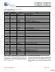
CY7C68013A, CY7C68014A CY7C68015A, CY7C68016A 5. Register Summary FX2LP register bit definitions are described in the FX2LP TRM in greater detail. Table 12.
CY7C68013A, CY7C68014A CY7C68015A, CY7C68016A Table 12. FX2LP Register Summary (continued) Hex E62B E62C E62D Size 1 1 1 Name ECC1B1 ECC1B2 ECC2B0 Description ECC1 Byte 1 Address ECC1 Byte 2 Address ECC2 Byte 0 Address b7 LINE7 COL5 LINE15 b6 LINE6 COL4 LINE14 b5 LINE5 COL3 LINE13 b4 LINE4 COL2 LINE12 b3 LINE3 COL1 LINE11 E62E E62F E630 H.S. E630 F.S. E631 H.S. E631 F.S E632 H.S. E632 F.S E633 H.S. E633 F.
CY7C68013A, CY7C68014A CY7C68015A, CY7C68016A Table 12.
CY7C68013A, CY7C68014A CY7C68015A, CY7C68016A Table 12.
CY7C68013A, CY7C68014A CY7C68015A, CY7C68016A Table 12.
CY7C68013A, CY7C68014A CY7C68015A, CY7C68016A Table 12.
CY7C68013A, CY7C68014A CY7C68015A, CY7C68016A Table 12.
CY7C68013A, CY7C68014A CY7C68015A, CY7C68016A 6. Absolute Maximum Ratings Storage Temperature ..................................................................................................................................................... 65°C to +150°C Ambient Temperature with Power Supplied (Commercial) ................................................................................................ 0°C to +70°C Ambient Temperature with Power Supplied (Industrial).....................................
CY7C68013A, CY7C68014A CY7C68015A, CY7C68016A 9. DC Characteristics Table 14. DC Characteristics Parameter VCC Description Conditions Supply Voltage VCC Ramp Up 0 to 3.3V Min Typ Max Unit 3.00 3.3 3.60 V μs 200 VIH Input HIGH Voltage 2 VIL Input LOW Voltage –0.5 0.8 V VIH_X Crystal Input HIGH Voltage 2 5.25 V VIL_X Crystal Input LOW Voltage II Input Leakage Current 0< VIN < VCC VOH Output Voltage HIGH IOUT = 4 mA VOL Output LOW Voltage IOUT = –4 mA 5.25 –0.5 V 0.
CY7C68013A, CY7C68014A CY7C68015A, CY7C68016A 10.2 Program Memory Read Figure 12. Program Memory Read Timing Diagram tCL CLKOUT[17] tAV tAV A[15..0] tSTBH tSTBL PSEN# [18] tACC1 D[7..0] tDH data in tSOEL OE# tSCSL CS# Table 15. Program Memory Read Parameters Parameter tCL Description Min 1/CLKOUT Frequency Typ Max 20.83 Unit Notes ns 48 MHz 41.66 ns 24 MHz 83.2 ns 12 MHz tAV Delay from Clock to Valid Address 0 10.
CY7C68013A, CY7C68014A CY7C68015A, CY7C68016A 10.3 Data Memory Read Figure 13. Data Memory Read Timing Diagram tCL Stretch = 0 CLKOUT[17] tAV tAV A[15..0] tSTBH tSTBL RD# tSCSL CS# tSOEL OE# tDSU [19] tDH tACC1 D[7..0] data in tCL Stretch = 1 CLKOUT[17] tAV A[15..0] RD# CS# tDSU tACC1[19] D[7..0] tDH data in Table 16. Data Memory Read Parameters Parameter tCL Description Min 1/CLKOUT Frequency Typ Max Unit Notes 20.83 ns 48 MHz 41.66 ns 24 MHz ns 12 MHz 83.
CY7C68013A, CY7C68014A CY7C68015A, CY7C68016A 10.4 Data Memory Write Figure 14. Data Memory Write Timing Diagram tCL CLKOUT tAV tSTBL tSTBH tAV A[15..0] WR# tSCSL CS# tON1 tOFF1 data out D[7..0] Stretch = 1 tCL CLKOUT tAV A[15..0] WR# CS# tON1 tOFF1 data out D[7..0] Table 17. Data Memory Write Parameters Min Max Unit tAV Parameter Delay from Clock to Valid Address Description 0 10.7 ns tSTBL Clock to WR Pulse LOW 0 11.2 ns tSTBH Clock to WR Pulse HIGH 0 11.
CY7C68013A, CY7C68014A CY7C68015A, CY7C68016A 10.5 PORTC Strobe Feature Timings The RD# and WR# are present in the 100-pin version and the 128-pin package. In these 100-pin and 128-pin versions, an 8051 control bit can be set to pulse the RD# and WR# pins when the 8051 reads from or writes to PORTC. This feature is enabled by setting PORTCSTB bit in CPUCS register. The RD# signal prompts the external logic to prepare the next data byte.
CY7C68013A, CY7C68014A CY7C68015A, CY7C68016A 10.6 GPIF Synchronous Signals Figure 17. GPIF Synchronous Signals Timing Diagram[20] tIFCLK IFCLK tSGA GPIFADR[8:0] RDYX tSRY tRYH DATA(input) valid tSGD tDAH CTLX tXCTL DATA(output) N N+1 tXGD Table 18. GPIF Synchronous Signals Parameters with Internally Sourced IFCLK[20, 21] Parameter Description Min Max 20.
CY7C68013A, CY7C68014A CY7C68015A, CY7C68016A 10.7 Slave FIFO Synchronous Read Figure 18. Slave FIFO Synchronous Read Timing Diagram[20] tIFCLK IFCLK tSRD tRDH SLRD tXFLG FLAGS DATA N tOEon N+1 tXFD tOEoff SLOE Table 20. Slave FIFO Synchronous Read Parameters with Internally Sourced IFCLK[21] Parameter Description Min Max Unit tIFCLK IFCLK Period 20.83 ns tSRD SLRD to Clock Setup Time 18.7 ns tRDH Clock to SLRD Hold Time 0 tOEon SLOE Turn-on to FIFO Data Valid 10.
CY7C68013A, CY7C68014A CY7C68015A, CY7C68016A 10.8 Slave FIFO Asynchronous Read Figure 19. Slave FIFO Asynchronous Read Timing Diagram[20] tRDpwh SLRD tRDpwl FLAGS tXFD tXFLG DATA N N+1 tOEon tOEoff SLOE Table 22.
CY7C68013A, CY7C68014A CY7C68015A, CY7C68016A 10.9 Slave FIFO Synchronous Write Figure 20. Slave FIFO Synchronous Write Timing Diagram[20] tIFCLK IFCLK SLWR DATA tSWR tWRH N Z tSFD Z tFDH FLAGS tXFLG Table 23. Slave FIFO Synchronous Write Parameters with Internally Sourced IFCLK[21] Parameter Description Min Max Unit tIFCLK IFCLK Period 20.83 ns tSWR SLWR to Clock Setup Time 10.4 ns tWRH Clock to SLWR Hold Time 0 ns tSFD FIFO Data to Clock Setup Time 9.
CY7C68013A, CY7C68014A CY7C68015A, CY7C68016A 10.10 Slave FIFO Asynchronous Write Figure 21. Slave FIFO Asynchronous Write Timing Diagram[20] tWRpwh SLWR SLWR/SLCS# tWRpwl tSFD tFDH DATA tXFD FLAGS Table 25.
CY7C68013A, CY7C68014A CY7C68015A, CY7C68016A There is no specific timing requirement that should be met for asserting PKTEND pin to asserting SLWR. PKTEND can be asserted with the last data value clocked into the FIFOs or thereafter. The setup time tSPE and the hold time tPEH must be met. caused the last byte or word to be clocked into the previous auto committed packet. Figure 23 shows this scenario. X is the value the AUTOINLEN register is set to when the IN endpoint is configured to be in auto mode.
CY7C68013A, CY7C68014A CY7C68015A, CY7C68016A 10.13 Slave FIFO Output Enable Figure 25. Slave FIFO Output Enable Timing Diagram[20] SLOE tOEoff tOEon DATA Table 29. Slave FIFO Output Enable Parameters Max Unit tOEon Parameter SLOE Assert to FIFO DATA Output Description Min 10.5 ns tOEoff SLOE Deassert to FIFO DATA Hold 10.5 ns 10.14 Slave FIFO Address to Flags/Data Figure 26. Slave FIFO Address to Flags/Data Timing Diagram[20] FIFOADR [1.0] tXFLG FLAGS tXFD DATA N N+1 Table 30.
CY7C68013A, CY7C68014A CY7C68015A, CY7C68016A 10.15 Slave FIFO Synchronous Address Figure 27. Slave FIFO Synchronous Address Timing Diagram[20] IFCLK SLCS/FIFOADR [1:0] tSFA tFAH Table 31. Slave FIFO Synchronous Address Parameters [21] Parameter Description Min Max Unit 20.83 200 ns tIFCLK Interface Clock Period tSFA FIFOADR[1:0] to Clock Setup Time 25 ns tFAH Clock to FIFOADR[1:0] Hold Time 10 ns 10.16 Slave FIFO Asynchronous Address Figure 28.
CY7C68013A, CY7C68014A CY7C68015A, CY7C68016A 10.17 Sequence Diagram 10.17.1 Single and Burst Synchronous Read Example Figure 29. Slave FIFO Synchronous Read Sequence and Timing Diagram[20] tIFCLK IFCLK tSFA tSFA tFAH tFAH FIFOADR t=0 tSRD T=0 tRDH >= tSRD >= tRDH SLRD t=3 t=2 T=3 T=2 SLCS tXFLG FLAGS tXFD tXFD Data Driven: N DATA N+1 N+1 N+2 N+3 tOEon tOEoff tOEon tXFD tXFD N+4 tOEoff SLOE t=4 T=4 T=1 t=1 Figure 30.
CY7C68013A, CY7C68014A CY7C68015A, CY7C68016A 10.17.2 Single and Burst Synchronous Write Figure 31.
CY7C68013A, CY7C68014A CY7C68015A, CY7C68016A 10.17.3 Sequence Diagram of a Single and Burst Asynchronous Read Figure 32. Slave FIFO Asynchronous Read Sequence and Timing Diagram[20] tSFA tFAH tSFA tFAH FIFOADR t=0 tRDpwl tRDpwh tRDpwl T=0 tRDpwl tRDpwh tRDpwl tRDpwh tRDpwh SLRD t=2 t=3 T=3 T=2 T=5 T=4 T=6 SLCS tXFLG tXFLG FLAGS tXFD Data (X) Driven DATA tXFD tXFD N N N+3 N+2 tOEon tOEoff tOEon tXFD N+1 tOEoff SLOE t=4 t=1 T=7 T=1 Figure 33.
CY7C68013A, CY7C68014A CY7C68015A, CY7C68016A 10.17.4 Sequence Diagram of a Single and Burst Asynchronous Write Figure 34.
CY7C68013A, CY7C68014A CY7C68015A, CY7C68016A 11. Ordering Information Table 33.
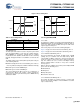
CY7C68013A, CY7C68014A CY7C68015A, CY7C68016A 12. Package Diagrams The FX2LP is available in five packages: ■ 56-pin SSOP ■ 56-pin QFN ■ 100-pin TQFP ■ 128-pin TQFP ■ 56-ball VFBGA Package Diagrams Figure 35. 56-lead Shrunk Small Outline Package O56 (51-85062) 51-85062-*C Document #: 38-08032 Rev.
CY7C68013A, CY7C68014A CY7C68015A, CY7C68016A Package Diagrams (continued) Figure 36. 56-Lead QFN 8 x 8 mm LF56A (51-85144) SIDE VIEW TOP VIEW BOTTOM VIEW 0.08[0.003] 7.90[0.311] 8.10[0.319] A C 1.00[0.039] MAX. 6.1 0.05[0.002] MAX. 7.70[0.303] 7.80[0.307] 0.18[0.007] 0.28[0.011] 0.80[0.031] MAX. 0.20[0.008] REF. N 1 2 2 6.1 0°-12° C SEATING PLANE 0.45[0.018] SOLDERABLE EXPOSED PAD 0.30[0.012] 0.50[0.020] 0.50[0.020] 6.45[0.254] 6.55[0.258] 6.45[0.254] 6.55[0.258] 7.70[0.303] 7.
CY7C68013A, CY7C68014A CY7C68015A, CY7C68016A Package Diagrams (continued) Figure 37. 100-Pin Thin Plastic Quad Flatpack (14 x 20 x 1.4 mm) A100RA (51-85050) 16.00±0.20 1.40±0.05 14.00±0.10 100 81 80 1 20.00±0.10 22.00±0.20 0.30±0.08 0.65 TYP. 30 12°±1° (8X) SEE DETAIL A 51 31 50 0.20 MAX. 0.10 1.60 MAX. R 0.08 MIN. 0.20 MAX. 0° MIN. SEATING PLANE STAND-OFF 0.05 MIN. 0.15 MAX. 0.25 NOTE: 1. JEDEC STD REF MS-026 GAUGE PLANE 0°-7° R 0.08 MIN. 0.20 MAX. 2.
CY7C68013A, CY7C68014A CY7C68015A, CY7C68016A Package Diagrams (continued) Figure 38. 128-Lead Thin Plastic Quad Flatpack (14 x 20 x 1.4 mm) A128 (51-85101) 16.00±0.20 14.00±0.10 1.40±0.05 128 1 20.00±0.10 22.00±0.20 0.22±0.05 12°±1° (8X) 0.50 TYP. SEE DETAIL A 0.20 MAX. 1.60 MAX. 0° MIN. 0.08 R 0.08 MIN. 0.20 MAX. STAND-OFF 0.05 MIN. 0.15 MAX. 0.25 GAUGE PLANE 0°-7° R 0.08 MIN. 0.20 MAX. SEATING PLANE NOTE: 1. JEDEC STD REF MS-026 2.
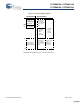
CY7C68013A, CY7C68014A CY7C68015A, CY7C68016A Package Diagrams (continued) Figure 39. 56 VFBGA (5 x 5 x 1.0 mm) 0.50 Pitch, 0.30 Ball BZ56 (001-03901) TOP VIEW BOTTOM VIEW Ø0.05 M C Ø0.15 M C A B PIN A1 CORNER A1 CORNER Ø0.30±0.05(56X) 8 7 6 5 4 3 2 1 A B C D E F G H 0.50 3.50 A B C D E F G H 5.00±0.10 5.00±0.10 1 2 3 4 5 6 6 8 0.50 -B3.50 -A- 5.00±0.10 5.00±0.10 0.080 C 0.45 SIDE VIEW 0.10 C 0.10(4X) REFERENCE JEDEC: MO-195C PACKAGE WEIGHT: 0.02 grams 0.160 ~0.260 1.
CY7C68013A, CY7C68014A CY7C68015A, CY7C68016A 14. Quad Flat Package No Leads (QFN) Package Design Notes Electrical contact of the part to the Printed Circuit Board (PCB) is made by soldering the leads on the bottom surface of the package to the PCB. Hence, special attention is required to the heat transfer area below the package to provide a good thermal bond to the circuit board. Design a Copper (Cu) fill in the PCB as a thermal pad under the package.
CY7C68013A, CY7C68014A CY7C68015A, CY7C68016A Document History Page Document Title: CY7C68013A, CY7C68014A, CY7C68015A, CY7C68016A, EZ-USB FX2LP™ USB Microcontroller High-Speed USB Peripheral Controller Document Number: 38-08032 REV. ECN NO. Issue Date Orig.
CY7C68013A, CY7C68014A CY7C68015A, CY7C68016A Document Title: CY7C68013A, CY7C68014A, CY7C68015A, CY7C68016A, EZ-USB FX2LP™ USB Microcontroller High-Speed USB Peripheral Controller Document Number: 38-08032 REV. ECN NO. Issue Date Orig. of Change MON Description of Change *K 420505 See ECN Remove SLCS from figure in Section 10.10. Removed indications that SLRD can be asserted simultaneously with SLCS in Section 10.17.2 and Section 10.17.