
High-Speed USB Peripheral Controller Specification Sheet


CY7C68013A, CY7C68014A
CY7C68015A, CY7C68016A
Document #: 38-08032 Rev. *L Page 26 of 62
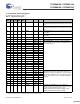
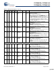
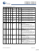
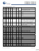
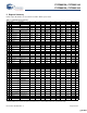
112 90 PE4 or
RXD1OUT
IO/Z I
(PE4)
Multiplexed pin whose function is selected by the
PORTECFG.4 bit.
PE4 is a bidirectional IO port pin.
RXD1OUT is an active-HIGH output from 8051 UART1.
When RXD1OUT is selected and UART1 is in Mode 0,
this pin provides the output data for UART1 only when
it is in sync mode. In Modes 1, 2, and 3, this pin is HIGH.
113 91 PE5 or
INT6
IO/Z I
(PE5)
Multiplexed pin whose function is selected by the
PORTECFG.5 bit.
PE5 is a bidirectional IO port pin.
INT6 is the 8051 INT6 interrupt request input signal. The
INT6 pin is edge-sensitive, active HIGH.
114 92 PE6 or
T2EX
IO/Z I
(PE6)
Multiplexed pin whose function is selected by the
PORTECFG.6 bit.
PE6 is a bidirectional IO port pin.
T2EX is an active-HIGH input signal to the 8051 Timer2.
T2EX reloads timer 2 on its falling edge. T2EX is active
only if the EXEN2 bit is set in T2CON.
115 93 PE7 or
GPIFADR8
IO/Z I
(PE7)
Multiplexed pin whose function is selected by the
PORTECFG.7 bit.
PE7 is a bidirectional IO port pin.
GPIFADR8 is a GPIF address output pin.
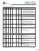
4 3 8 1 1A RDY0 or
SLRD
Input N/A Multiplexed pin whose function is selected by the
following bits:
IFCONFIG[1..0].
RDY0 is a GPIF input signal.
SLRD is the input-only read strobe with programmable
polarity (FIFOPINPOLAR.3) for the slave FIFOs
connected to FD[7..0] or FD[15..0].
5 4 9 2 1B RDY1 or
SLWR
Input N/A Multiplexed pin whose function is selected by the
following bits:
IFCONFIG[1..0].
RDY1 is a GPIF input signal.
SLWR is the input-only write strobe with programmable
polarity (FIFOPINPOLAR.2) for the slave FIFOs
connected to FD[7..0] or FD[15..0].
6 5 RDY2 Input N/A RDY2 is a GPIF input signal.
7 6 RDY3 Input N/A RDY3 is a GPIF input signal.
8 7 RDY4 Input N/A RDY4 is a GPIF input signal.
9 8 RDY5 Input N/A RDY5 is a GPIF input signal.
69 54 36 29 7H CTL0 or
FLAGA
O/Z H Multiplexed pin whose function is selected by the
following bits:
IFCONFIG[1..0].
CTL0 is a GPIF control output.
FLAGA is a programmable slave-FIFO output status
flag signal.
Defaults to programmable for the FIFO selected by the
FIFOADR[1:0] pins.
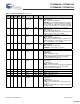
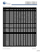
Table 11. FX2LP Pin Descriptions (continued)
128
TQFP
100
TQFP
56
SSOP
56
QFN
56 VF-
BGA
Name Type Default Description
[+] Feedback [+] Feedback