
nvSRAM Specification Sheet

STK14D88
Document Number: 001-52037 Rev. ** Page 2 of 17
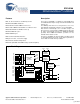
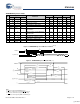
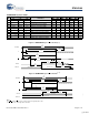
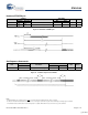
Pin Configurations
Figure 1. Pin Diagram 48-Pin SSOP/32-SOIC
Pin Descriptions
Pin Name I/O Description
A
14
-A
0
Input Address: The 15 address inputs select one of 32,768 bytes in the nvSRAM array
DQ
7
-DQ
0
I/O Data: Bi-directional 8-bit data bus for accessing the nvSRAM
E
Input Chip Enable: The active low E input selects the device
W
Input Write Enable: The active low W enables data on the DQ pins to be written to the address location
latched by the falling edge of E
G Input Output Enable: The active low G input enables the data output buffers during read cycles.
De-asserting G
high caused the DQ pins to tri-state.
V
CC
Power Supply Power: 3.0V, +20%, -10%
HSB
I/O Hardware Store Busy: When low this output indicates a Store is in progress. When pulled low
external to the chip, it will initiate a nonvolatile STORE operation. A weak pull up resistor keeps this
pin high if not connected. (Connection Optional).
V
CAP
Power Supply AutoStore™ Capacitor: Supplies power to nvSRAM during power loss to store data from SRAM to
nonvolatile storage elements.
V
SS
Power Supply Ground
NC No Connect Unlabeled pins have no internal connections.
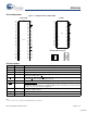
48-Pin SSOP
TOP
V
SS
A
14
A
12
A
7
A
6
DQ
0
DQ
1
V
CC
DQ
2
A
3
A
2
A
1
V
CAP
A
13
A
8
A
9
A
11
A
10
DQ
7
DQ
6
V
SS
A
0
NC
44
43
42
41
40
39
38
37
36
35
34
33
32
31
30
29
28
27
26
25
1
2
3
4
5
6
7
8
9
10
11
12
13
14
15
16
17
18
19
20
21
22
NC
E
NC
NC
23
24
A
5
NC
NC
NC
NC
NC
NC
A
4
48
47
46
45
V
CC
HSB
NC
NC
W
NC
NC
DQ
5
DQ
3
DQ
4
G
NC NC
32-SOIC
TOP
V
SS
A
14
A
12
A
7
A
6
DQ
0
V
CAP
A
13
A
8
A
9
A
11
28
27
26
25
24
23
22
21
20
19
18
17
1
2
3
4
5
6
7
8
9
10
11
12
13
14
15
16
A
5
A
4
32
31
30
29
V
CC
HSB
W
A
3
A
2
A
1
A
0
DQ
1
DQ
2
A
10
DQ
7
DQ
5
DQ
3
DQ
4
DQ
6
NCNC
E
G
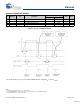
SSOP
Relative PCB Area Usage
[1]
Note
1. See “Package Diagrams” on page 15 for detailed package size specifications.
[+] Feedback