
Independent Clock Deserializing Reclocker Specification Sheet

CYV15G0404RB
Document #: 38-02102 Rev. *C Page 10 of 27
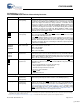
DATA[7:0] LVTTL input
asynchronous,
internal pull-up
Control Data Bus. The DATA[7:0] bus is the input data bus that configures the
device. The WREN
input writes the values of the DATA[7:0] bus into the latch
specified by address location on the ADDR[3:0] bus.
[3]
Table 3, “Device Configu-
ration and Control Latch Descriptions,” on page 14 lists the configuration latches
within the device, and the initialization value of the latches when RESET is
asserted. Table 4, “Device Control Latch Configuration Table,” on page 16 shows
the way the latches are mapped in the device.
Internal Device Configuration Latches
RXRATE[A..D] Internal Latch
[4]
Receive Clock Rate Select.
SDASEL[2..1][A..D]
[1:0]
Internal Latch
[4]
Signal Detect Amplitude Select.
RXPLLPD[A..D] Internal Latch
[4]
Receive Channel Power Control.
RXBIST[A..D][1:0] Internal Latch
[4]
Receive BIST Disabled.
ROE2[A..D] Internal Latch
[4]
Reclocker Differential Serial Output Driver 2 Enable.
ROE1[A..D] Internal Latch
[4]
Reclocker Differential Serial Output Driver 1 Enable.
GLEN[11..0] Internal Latch
[4]
Global Latch Enable.
FGLEN[2..0] Internal Latch
[4]
Force Global Latch Enable.
Factory Test Modes
SCANEN2 LVTTL input,
internal pull down
Factory Test 2. The SCANEN2 input is for factory testing only. Leave this input
as a NO CONNECT, or GND only.
TMEN3 LVTTL input,
internal pull down
Factory Test 3. The TMEN3 input is for factory testing only. Leave this input as a
NO CONNECT, or GND only.
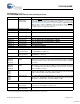
Analog I/O
ROUTA1±
ROUTB1±
ROUTC1±
ROUTD1±
CML Differential
Output
Primary Differential Serial Data Output. The ROUTx1± PECL-compatible CML
outputs (+3.3V referenced) can drive terminated transmission lines or standard
fiber-optic transmitter modules, and must be AC-coupled for PECL-compatible
connections.
ROUTA2±
ROUTB2±
ROUTC2±
ROUTD2±
CML Differential
Output
Secondary Differential Serial Data Output. The ROUTx2± PECL-compatible
CML outputs (+3.3V referenced) are capable of driving terminated transmission
lines or standard fiber-optic transmitter modules, and must be AC coupled for
PECL-compatible connections.
INA1±
INB1±
INC1±
IND1±
Differential Input Primary Differential Serial Data Input. The INx1± input accepts the serial data
stream for deserialization. The INx1± serial stream passes to the receive CDR
circuit to extract the data content when INSELx = HIGH.
INA2±
INB2±
INC2±
IND2±
Differential Input Secondary Differential Serial Data Input. The INx2± input accepts the serial
data stream for deserialization. The INx2± serial stream passes to the receiver
CDR circuit to extract the data content when INSELx = LOW.
JTAG Interface
TMS LVTTL Input,
internal pull up
Test Mode Select. Controls access to the JTAG Test Modes. If TMS is HIGH for
>
5 TCLK cycles, the JTAG test controller resets.
TCLK LVTTL Input,
internal pull down
JTAG Test Clock.
Note
4. See Device Configuration and Control Interface for detailed information on the internal latches.
Pin Definitions (continued)
CYV15G0404RB Quad HOTLink II Deserializing Reclocker
Name IO Characteristics Signal Description
[+] Feedback