
Independent Clock Deserializing Reclocker Specification Sheet


CYV15G0404RB
Document #: 38-02102 Rev. *C Page 12 of 27
operates at, or near the rate of the incoming data stream for
two primary cases:
• When the incoming data stream resumes after a time in
which it was “missing.”
• When the incoming data stream is outside the acceptable
signaling rate range.
To perform this function, periodically compare the frequency of
the RXPLL VCO to the frequency of the TRGCLKx± input. If
the VCO is running at a frequency beyond ±1500 ppm
[21]
as
defined by the TRGCLKx± frequency, it is periodically forced
to the correct frequency (as defined by TRGCLKx±, SPDSELx,
and TRGRATEx) and then released in an attempt to lock to the
input data stream.
Calculate the sampling and relock period of the Range Control
as follows: RANGE_CONTROL_SAMPLING_PERIOD =
(RECOVERED BYTE CLOCK PERIOD) * (4096).
During the time that the Range Control forces the RXPLL VCO
to track TRGCLKx±, the LFIx
output is asserted LOW. After a
valid serial data stream is applied, it may take up to one
RANGE CONTROL SAMPLING PERIOD before the PLL
locks to the input data stream, after which LFIx
is HIGH.
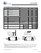
Table 2 lists the operating serial signaling rate and allowable
range of TRGCLK± frequencies.
Receive Channel Enabled
The CYV15G0404RB contains four receive channels that it
can independently enable and disable. Each channel are
enabled or disabled separately through the RXPLLPDx input
latch as controlled by the device configuration interface.
RXPLLPDx latch = 0 disables the associated PLL and analog
circuitry of the channel. Any disabled channel indicates a
constant link fault condition on the LFIx output. RXPLLPDx =
1 enables the associated PLL and receive channel to receive
a serial stream.
Note When a disabled receive channel is reenabled, the
status of the associated LFIx
output and data on the parallel
outputs for the associated channel may be indeterminate for
up to 2 ms.
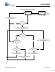
Clock/Data Recovery
A separate CDR block within each receive channel performs
the extraction of a bit rate clock and recovery of bits from each
received serial stream. An integrated PLL that tracks the
frequency of the transitions in the incoming bit stream and
aligns the phase of the internal bit rate clock to the transitions
in the selected serial data stream performs the clock extraction
function.
Each CDR accepts a character-rate (bit-rate ÷ 10) or
half-character-rate (bit-rate ÷ 20) training clock from the
associated TRGCLKx± input. This TRGCLKx± input is used to
• Ensure that the VCO (within the CDR) is operating at the
correct frequency (rather than a harmonic of the bit rate)
• Reduce PLL acquisition time
• Limit unlocked frequency excursions of the CDR VCO when
there is no input data present at the selected Serial Line
Receiver.
Regardless of the type of signal present, the CDR attempts to
recover a data stream from it. If the signaling rate of the
recovered data stream is outside the limits set by the range
control monitors, the CDR tracks TRGCLKx± instead of the
data stream. Once the CDR output (RXCLK±) frequency
returns close to TRGCLKx± frequency, the CDR input
switches back to the input data stream. If no data is present at
the selected line receiver, this switching behavior may cause
brief RXCLK± frequency excursions from TRGCLKx±.
However, the LFIx
output indicates the validity of the input data
stream. The frequency of TRGCLKx± must be within ±1500
ppm
[21]
of the frequency of the clock that drives the reference
clock input of the remote transmitter, to ensure a lock to the
incoming data stream. This large ppm tolerance allows the
CDR PLL to reliably receive a 1.485 or 1.485/1.001 Gbps
SMPTE HD-SDI data stream with a constant TRGCLK
frequency.
For systems using multiple or redundant connections, use the
LFIx output to select an alternate data stream. When the
device detects an LFIx
indication, external logic toggles
selection of the associated INx1± and INx2± input through the
associated INSELx input. When a port switch takes place, the
receive PLL for that channel reacquires the new serial stream.
Reclocker
Each receive channel performs a reclocker function on the
incoming serial data. To do this, the Clock and Data Recovery
PLL first recovers the clock from the data. The recovered clock
retimes the data and then passes it to an output register. It also
passes the recovered character clock from the receive PLL to
the reclocker output PLL, which generates the bit clock that
clocks the retimed data into the output register. This data
stream is then transmitted through the differential serial
outputs.
Reclocker Serial Output Drivers
The serial output interface drivers use differential Current
Mode Logic (CML) drivers to provide source-matched drivers
for 50Ω transmission lines. These drivers accept data from the
reclocker output register in the reclocker channel. These
drivers have signal swings equivalent to that of standard PECL
drivers, and can drive AC coupled optical modules or trans-
mission lines.
Reclocker Output Channels Enabled
Each driver can be enabled or disabled separately via the
device configuration interface.
When a driver is disabled using the configuration interface, it
internally powers down to reduce device power. If both
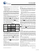
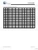
Table 2. Operating Speed Settings
SPDSELx TRGRATEx
TRGCLKx±
Frequency
(MHz)
Signaling
Rate (Mbps)
LOW
1 Reserved 195–400
0 19.5–40
MID (Open) 1 20–40 400–800
0 40–80
HIGH 1 40–75 800–1500
0 80–150
[+] Feedback