
Independent Clock Deserializing Reclocker Specification Sheet


CYV15G0404RB
Document #: 38-02102 Rev. *C Page 13 of 27
reclocker serial drivers for a channel are in this disabled state,
the associated internal reclocker logic also powers down. The
deserialization logic and parallel outputs remain enabled. A
device reset (RESET sampled LOW) disables all output
drivers.
Note When the disabled reclocker function (that is, both
outputs disabled) is reenabled, the data on the reclocker serial
outputs may not meet all timing specifications for up to 250 µs.
Output Bus
Each receive channel presents a 10-bit data signal (and a
BIST status signal when RXBISTx[1:0] = 10).
Receive BIST Operation
Each receiver channel contains an internal pattern checker
that is used to validate both device and link operation. These
pattern checkers are enabled by the associated RXBISTx[1:0]
latch through the device configuration interface. When
enabled, a register in the associated receive channel becomes
a signature pattern generator and checker by logically
converting to a Linear Feedback Shift Register (LFSR). This
LFSR generates a 511-character sequence. This provides a
predictable, yet pseudorandom, sequence that can be
matched to an identical LFSR in the attached Transmitter(s).
When synchronized with the received data stream, the
associated Receiver checks each character from the deseri-
alizer with each character generated by the LFSR and
indicates compare errors and BIST status at the RXDx[1:0]
and BISTSTx bits of the Output Register.
The BIST status bus {BISTSTx, RXDx[0], RXDx[1]} indicates
010b or 100b for one character period per BIST loop to
indicate loop completion. Use this status to check test pattern
progress.
Table 5, “Receive BIST Status Bits,” on page 17 lists the
specific status reported by the BIST state machine. The
receive status outputs report these same codes.
If the number of invalid characters received exceeds the
number of valid characters by 16, the receive BIST state
machine aborts the compare operations and resets the LFSR
to look for the start of the BIST sequence again.
A device reset (RESET
sampled LOW) presets the BIST
Enable Latches to disable BIST on all channels.
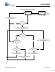
BIST Status State Machine
When a receive path is enabled to look for and compare the
received data stream with the BIST pattern, the {BISTSTx,
RXDx[0], RXDx[1]} bits identify the present state of the BIST
compare operation.
The BIST state machine has multiple states, as shown in
Figure 2, "Receive BIST State Machine," on page 18 and
Table 5, “Receive BIST Status Bits,” on page 17. When the
receive PLL detects an out-of-lock condition, it forces the BIST
state to the Start-of-BIST state, regardless of the present state
of the BIST state machine. If the number of detected errors
ever exceeds the number of valid matches by greater than 16,
the state machine is forced to the WAIT_FOR_BIST state,
where it monitors the receive path for the first character of the
next BIST sequence.
Power Control
The CYV15G0404RB supports user control of the powered up
or down state of each transmit and receive channel. The
RXPLLPDx latch controls the receive channels through the
device configuration interface. RXPLLPDx = 0 disables the
associated PLL and analog circuitry of the channel. The OE1x
and the OE2x latches control the transmit channels via the
device configuration interface. The ROE1x and the ROE2x
latches control the reclocker function through the device
configuration interface. When the configuration interface
disables a driver, the driver internally powers down to reduce
device power. If both serial drivers for a channel are in this
disabled state, the associated internal logic for that channel
also powers down. The reclocker serial drivers being disabled
in turn disables the reclocker function, but the deserialization
logic and parallel outputs remain enabled.
Device Reset State
Assertion of RESET
resets all state machines, counters, and
configuration latches in the device to a reset state.
Additionally, the JTAG controller must be reset for valid
operation (even if not performing JTAG testing). See “JTAG
Support” on page 17 for JTAG state machine initialization. See
Table 3, “Device Configuration and Control Latch Descrip-
tions,” on page 14 for the initialize values of the configuration
latches.
Following a device reset, enable the receive channels used for
normal operation. Do this by sequencing the appropriate
values on the device configuration interface.
[3]
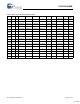
Device Configuration and Control Interface
Configure the CYV15G0404RB through the configuration
interface. The configuration interface enables the device to be
configured globally or enables each channel to be configured
independently. Table 3, “Device Configuration and Control
Latch Descriptions,” on page 14 lists the configuration latches
within the device, including the initialization value of the
latches on the assertion of RESET
. Table 4, “Device Control
Latch Configuration Table,” on page 16 shows how the latches
are mapped in the device. Each row in Table 4 maps to an 8-bit
latch bank. There are 16 such write only latch banks. When
WREN
= 0, the logic value in the DATA[7:0] latches to the latch
bank specified by the values in ADDR[3:0]. The second
column of Table 4 specifies the channels associated with the
corresponding latch bank. For example, the first three latch
banks (0, 1, and 2) consist of configuration bits for channel A.
Latch banks 12, 13, and 14 consist of Global configuration bits,
and the last latch bank (15) is the Mask latch bank, which can
be configured to perform bit-by-bit configuration.
Global Enable Function
The global enable function, controlled by the GLENx bits, is a
feature that can reduce the number of write operations needed
to set up the latch banks. This function is beneficial in systems
that use a common configuration in multiple channels. The
GLENx bit is present in bit 0 of latch banks 0 through 11 only.
Its default value (1) enables the global update of the latch
bank's contents. Setting the GLENx bit to 0 disables this
functionality.
[+] Feedback