
Independent Clock Deserializing Reclocker Specification Sheet


CYV15G0404RB
Document #: 38-02102 Rev. *C Page 14 of 27
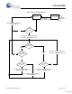
Latch Banks 12, 13, and 14 load values in the related latch
banks in globally. A write operation to latch bank 12 performs
a global write to latch banks 0, 3, 6, and 9, depending on the
value of GLENx in these latch banks; latch bank 13 performs
a global write to latch banks 1, 4, 7, and 10; and latch bank 14
performs a global write to latch banks 2, 5, 8, and 11. The
GLENx bit cannot be modified by a global write operation.
Force Global Enable Function
FGLENx forces the global update of the target latch banks, but
does not change the contents of the GLENx bits. If FGLENx =
1 for the associated global channel, FGLENx forces the global
update of the target latch banks.
Mask Function
An additional latch bank (15) is a global mask vector that
controls the update of the configuration latch banks on a
bit-by-bit basis. A logic 1 in a bit location enables the update
of that same location of the target latch bank(s), whereas a
logic 0 disables it. The reset value of this latch bank is FFh,
thereby making its use optional by default. The mask latch
bank is not maskable. The bit 0 value of the mask latch bank
does not affect the FGLEN functionality.
Latch Types
There are two types of latch banks: static (S) and dynamic (D).
Each channel is configured by two static and one dynamic
latch banks. The S type contains those settings that normally
do not change for a given application, whereas the D type
controls the settings that might change during the application's
lifetime. The first and second rows of each channel (address
numbers 0, 1, 3, 4, 6, 7, 9, and 10) are the static control
latches. The third row of latches for each channel (address
numbers 2, 5, 8, and 11) are the dynamic control latches that
are associated with enabling dynamic functions within the
device.
Latch Bank 14 is also useful for those users that do not need
the latch based programmable feature of the device. This latch
bank is used in those applications that do not need to modify
the default value of the static latch banks, and that can afford
global (that is, not independent) control of the dynamic signals.
In this case, this feature becomes available when ADDR[3:0]
is unchanged with a value of “1110” and WREN
is asserted.
The signals present in DATA[7:0] effectively become global
control pins, and for the latch banks 2, 5, 8, and 11.
Static Latch Values
There are some latches in the table that have a static value
(that is, 1, 0, or X). The latches that have a ‘1’ or ‘0’ must be
configured with their corresponding value each time that their
associated latch bank is configured. The latches that have an
‘X’ are don’t cares and can be configured with any value
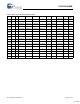
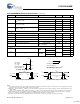
Table 3. Device Configuration and Control Latch Descriptions
Name Signal Description
RXRATEA
RXRATEB
RXRATEC
RXRATED
Receive Clock Rate Select. The initialization value of the RXRATEx latch = 1. RXRATEx selects the rate
of the RXCLKx± clock output.
When RXRATEx = 1, the RXCLKx± clock outputs are complementary clocks that follow the recovered
clock operating at half the character rate. Data for the associated receive channels must latch alternately
on the rising edge of RXCLKx+ and RXCLKx–.
When RXRATEx = 0, the RXCLKx± clock outputs are complementary clocks that follow the recovered
clock operating at the character rate. Data for the associated receive channels must latch on the rising
edge of RXCLKx+ or falling edge of RXCLKx–.
SDASEL1A[1:0]
SDASEL1B[1:0]
SDASEL1C[1:0]
SDASEL1D[1:0]
Primary Serial Data Input Signal Detector Amplitude Select. The initialization value of the
SDASEL1x[1:0] latch = 10. SDASEL1x[1:0] selects the trip point for the detection of a valid signal for the
INx1± Primary Differential Serial Data Inputs.
When SDASEL1x[1:0] = 00, the Analog Signal Detector is disabled.
When SDASEL1x[1:0] = 01, the typical p-p differential voltage threshold level is 140 mV.
When SDASEL1x[1:0] = 10, the typical p-p differential voltage threshold level is 280 mV.
When SDASEL1x[1:0] = 11, the typical p-p differential voltage threshold level is 420 mV.
SDASEL2A[1:0]
SDASEL2B[1:0]
SDASEL2C[1:0]
SDASEL2D[1:0]
Secondary Serial Data Input Signal Detector Amplitude Select. The initialization value of the
SDASEL2x[1:0] latch = 10. SDASEL2x[1:0] selects the trip point for the detection of a valid signal for the
INx2± Secondary Differential Serial Data Inputs.
When SDASEL2x[1:0] = 00, the Analog Signal Detector is disabled
When SDASEL2x[1:0] = 01, the typical p-p differential voltage threshold level is 140 mV.
When SDASEL2x[1:0] = 10, the typical p-p differential voltage threshold level is 280 mV.
When SDASEL2x[1:0] = 11, the typical p-p differential voltage threshold level is 420 mV.
TRGRATEA
TRGRATEB
TRGRATEC
TRGRATED
Training Clock Rate Select. The initialization value of the TRGRATEx latch = 0. TRGRATEx selects the
clock multiplier for the training clock input to the associated CDR PLL. When TRGRATEx = 0, the
associated TRGCLKx± input is not multiplied before it is passed to the CDR PLL. When TRGRATEx = 1,
the TRGCLKx± input is multiplied by 2 before it is passed to the CDR PLL. TRGRATEx = 1 and SPDSELx
= LOW is an invalid state and this combination is reserved.
[+] Feedback