
Independent Clock Deserializing Reclocker Specification Sheet


CYV15G0404RB
Document #: 38-02102 Rev. *C Page 15 of 27
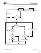
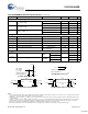
Device Configuration Strategy
Follow these steps to load the configuration latches on each
channel:
1. Pulse RESET
Low after device power up. This operation
resets all four channels. Initialize the JTAG state machine
to its reset state, as detailed in “JTAG Support” on page 17.
2. Set the static latch banks for the target channel. You can
perform this step using a global operation, if the application
permits it. [This is an optional step if the default settings
match the desired configuration.]
3. Set the dynamic bank of latches for the target channel.
Enable the Receive PLLs and set each channel for SMPTE
data reception (RXBISTx[1:0] = 01) or BIST data reception
(RXBISTx[1:0] = 10). You can perform this step using a
global operation, if the application permits it. [Required
step.]
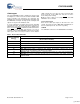
RXPLLPDA
RXPLLPDB
RXPLLPDC
RXPLLPDD
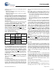
Receive Channel Enable. The initialization value of the RXPLLPDx latch = 0. RXPLLPDx selects whether
the associated receive channel is enabled or powered down. RXPLLPDx = 0 powers down the associated
receive PLL and analog circuitry. RXPLLPDx = 1 enables the associated receive PLL and analog circuitry.
RXBISTA[1:0]
RXBISTB[1:0]
RXBISTC[1:0]
RXBISTD[1:0]
Receive Bist Disable / SMPTE Receive Enable. The initialization value of the RXBISTx[1:0] latch = 11.
For SMPTE data reception, RXBISTx[1:0] should not remain in this initialization state (11). RXBISTx[1:0]
selects whether receive BIST is disabled or enabled and sets the associated channel for SMPTE data
reception. RXBISTx[1:0] = 01 disables the receiver BIST function and sets the associated channel to
receive SMPTE data. RXBISTx[1:0] = 10 enables the receive BIST function and sets the associated
channel to receive BIST data. RXBISTx[1:0] = 00 and RXBISTx[1:0] = 11 are invalid states.
ROE2A
ROE2B
ROE2C
ROE2D
Reclocker Secondary Differential Serial Data Output Driver Enable. The initialization value of the
ROE2x latch = 0. ROE2x selects whether the ROUT2± secondary differential output drivers are enabled
or disabled. ROE2x = 1 enables the associated serial data output driver, allowing data to be transmitted
from the transmit shifter. ROE2x = 0 disables the associated serial data output driver. When the config-
uration interface disables a driver, the driver internally powers down to reduce device power. If both serial
drivers for a channel are in this disabled state, the associated internal logic for that channel also powers
down. A device reset (RESET sampled LOW) disables all output drivers.
ROE1A
ROE1B
ROE1C
ROE1D
Reclocker Primary Differential Serial Data Output Driver Enable. The initialization value of the ROE1x
latch = 0. ROE1x selects whether the ROUT1± primary differential output drivers are enabled or disabled.
ROE1x = 1 enables the associated serial data output driver, allowing data to be transmitted from the
transmit shifter. ROE1x = 0 disables the associated serial data output driver. When the configuration
interface disables a driver, the driver internally powers down to reduce device power. If both serial drivers
for a channel are in this disabled state, the associated internal logic for that channel also powers down.
A device reset (RESET sampled LOW) disables all output drivers.
GLEN[11..0] Global Enable. The initialization value of the GLENx latch = 1. The GLENx reconfigures several channels
simultaneously in applications where several channels may have the same configuration. When GLENx
= 1 for a given address, that address can participate in a global configuration. When GLENx = 0 for a
given address, that address cannot participate in a global configuration.
FGLEN[2..0] Force Global Enable. The initialization value of the FGLENx latch is NA. The FGLENx latch forces a
GLobal ENable no matter what the setting is on the GLENx latch. If FGLENx = 1 for the associated Global
channel, FGLEN forces the global update of the target latch banks.
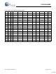
Table 3. Device Configuration and Control Latch Descriptions (continued)
Name Signal Description
[+] Feedback