
Independent Clock Deserializing Reclocker Specification Sheet


CYV15G0404RB
Document #: 38-02102 Rev. *C Page 19 of 27
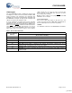
Maximum Ratings
Excedding maximum ratings may shorten the device life. User
guidelines are not tested
Storage Temperature ..................................–65°C to +150°C
Ambient Temperature with
Power Applied.............................................–55°C to +125°C
Supply Voltage to Ground Potential ............... –0.5V to +3.8V
DC Voltage Applied to LVTTL Outputs
in High-Z State .......................................–0.5V to V
CC
+ 0.5V
Output Current into LVTTL Outputs (LOW)..................60 mA
DC Input Voltage....................................–0.5V to V
CC
+ 0.5V
Static Discharge Voltage..........................................> 2000 V
(MIL-STD-883, Method 3015)
Latch Up Current ....................................................> 200 mA
Power Up Requirements
The CYV15G0404RB requires one power supply. The voltage
on any input or I/O pin cannot exceed the power pin during
power up.
Operating Range
Range Ambient Temperature V
CC
Commercial 0°C to +70°C +3.3V ±5%
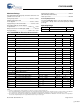
Notes
6. Tested one output at a time, output shorted for less than one second, less than 10% duty cycle.
7. This is the minimum difference in voltage between the true and complement inputs required to ensure detection of a logic-1 or logic-0. A logic-1 exists when the
true (+) input is more positive than the complement (−) input. A logic-0 exists when the complement (−) input is more positive than true (+) input.
8. The common mode range defines the allowable range of TRGCLKx+ and TRGCLKx− when TRGCLKx+ = TRGCLKx−. This marks the zero-crossing between
the true and complement inputs as the signal switches between a logic-1 and a logic-0.
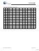
CYV15G0404RB DC Electrical Characteristics
Parameter Description Test Conditions Min Max Unit
LVTTL-compatible Outputs
V
OHT
Output HIGH Voltage I
OH
= −4 mA, V
CC
= Min. 2.4 V
V
OLT
Output LOW Voltage I
OL
= 4 mA, V
CC
= Min. 0.4 V
I
OST
Output Short Circuit Current V
OUT
= 0V
[6]
, V
CC
= 3.3V –20 –100 mA
I
OZL
High-Z Output Leakage Current V
OUT
= 0V, V
CC
–20 20 µA
LVTTL-compatible Inputs
V
IHT
Input HIGH Voltage 2.0 V
CC
+ 0.3 V
V
ILT
Input LOW Voltage –0.5 0.8 V
I
IHT
Input HIGH Current TRGCLKx Input, V
IN
= V
CC
1.5 mA
Other Inputs, V
IN
= V
CC
+40 µA
I
ILT
Input LOW Current TRGCLKx Input, V
IN
= 0.0V –1.5 mA
Other Inputs, V
IN
= 0.0V –40 µA
I
IHPDT
Input HIGH Current with Internal Pull Down V
IN
= V
CC
+200 µA
I
ILPUT
Input LOW Current with Internal Pull Up V
IN
= 0.0V –200 µA
LVDIFF Inputs: TRGCLKx±
V
DIFF
[7]
Input Differential Voltage 400 V
CC
mV
V
IHHP
Highest Input HIGH Voltage 1.2 V
CC
V
V
ILLP
Lowest Input LOW voltage 0.0 V
CC
/2 V
V
COMREF
[8]
Common Mode Range 1.0 V
CC
– 1.2V V
3-Level Inputs
V
IHH
Three-Level Input HIGH Voltage Min. ≤ V
CC
≤ Max. 0.87 * V
CC
V
CC
V
V
IMM
Three-Level Input MID Voltage Min. ≤ V
CC
≤ Max. 0.47 * V
CC
0.53 * V
CC
V
V
ILL
Three-Level Input LOW Voltage Min. ≤ V
CC
≤ Max. 0.0 0.13 * V
CC
V
I
IHH
Input HIGH Current V
IN
= V
CC
200 µA
I
IMM
Input MID current V
IN
= V
CC
/2 –50 50 µA
I
ILL
Input LOW current V
IN
= GND –200 µA
[+] Feedback