
Independent Clock Deserializing Reclocker Specification Sheet

CYV15G0404RB
Document #: 38-02102 Rev. *C Page 21 of 27
Notes
14. Tested initially and after any design or process changes that may affect these parameters, but not 100% tested.
15. The ratio of rise time to falling time must not vary by greater than 2:1.
16. For a given operating frequency, neither rise nor fall specification can be greater than 20% of the clock cycle period or the data sheet maximum time.
17. All transmit AC timing parameters measured with 1ns typical rise time and fall time.
18. Parallel data output specifications are only valid if all outputs are loaded with similar DC and AC loads.
19. Receiver UI (Unit Interval) is calculated as 1/(f
TRG
* 20) (when TRGRATEx = 1) or 1/(f
TRG
* 10) (when TRGRATEx = 0). In an operating link this is equivalent to t
B
.
20. The duty cycle specification is a simultaneous condition with the t
REFH
and t
REFL
parameters. This means that at faster character rates the TRGCLKx± duty
cycle cannot be as large as 30%–70%.
21. TRGCLKx± has no phase or frequency relationship with the recovered clock(s) and only acts as a centering reference to reduce clock synchronization time.
TRGCLKx± must be within ±1500 PPM (±0.15%) of the transmitter PLL reference (REFCLKx±) frequency. Although transmitting to a HOTLink II receiver channel
necessitates the frequency difference between the transmitter and receiver reference clocks to be within ±1500-PPM, the stability of the crystal needs to be
within the limits specified by the appropriate standard when transmitting to a remote receiver that is compliant to that standard.
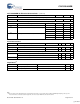
CYV15G0404RB AC Electrical Characteristics
Parameter Description Min Max Unit
CYV15G0404RB Receiver LVTTL Switching Characteristics Over the Operating Range
f
RS
RXCLKx± Clock Output Frequency 9.75 150 MHz
t
RXCLKP
RXCLKx± Period = 1/f
RS
6.66 102.56 ns
t
RXCLKD
RXCLKx± Duty Cycle Centered at 50% (Full Rate and Half Rate) –1.0 +1.0 ns
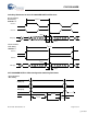
t
RXCLKR
[14]
RXCLKx± Rise Time 0.3 1.2 ns
t
RXCLKF
[14]
RXCLKx± Fall Time 0.3 1.2 ns
t
RXDv–
[18]
Status and Data Valid Time to RXCLKx± (RXRATEx = 0) (Full Rate) 5UI–2.0
[19]
ns
Status and Data Valid Time to RXCLKx± (RXRATEx = 1) (Half Rate) 5UI–1.3
[19]
ns
t
RXDv+
[18]
Status and Data Valid Time to RXCLKx± (RXRATEx = 0) 5UI–1.8
[19]
ns
Status and Data Valid Time to RXCLKx± (RXRATEx = 1) 5UI–2.6
[19]
ns
f
ROS
RECLKOx Clock Frequency 19.5 150 MHz
t
RECLKO
RECLKOx Period = 1/f
ROS
6.66 51.28 ns
t
RECLKOD
RECLKOx Duty Cycle centered at 60% HIGH time –1.9 0 ns
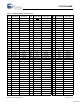
CYV15G0404RB TRGCLKx Switching Characteristics Over the Operating Range
f
TRG
TRGCLKx Clock Frequency 19.5 150 MHz
TRGCLK
TRGCLKx Period = 1/f
REF
6.6 51.28 ns
t
TRGH
TRGCLKx HIGH Time (TRGRATEx = 1)(Half Rate) 5.9 ns
TRGCLKx HIGH Time (TRGRATEx = 0)(Full Rate) 2.9
[14]
ns
t
TRGL
TRGCLKx LOW Time (TRGRATEx = 1)(Half Rate) 5.9 ns
TRGCLKx LOW Time (TRGRATEx = 0)(Full Rate) 2.9
[14]
ns
t
TRGD
[20]
TRGCLKx Duty Cycle 30 70 %
t
TRGR
[14, 15, 16, 17]
TRGCLKx Rise Time (20%–80%) 2 ns
t
TRGF
[14, 15, 16, 17]
TRGCLKx Fall Time (20%–80%) 2 ns
t
TRGRX
[21]
TRGCLKx Frequency Referenced to Received Clock Frequency –0.15 +0.15 %
CYV15G0404RB Bus Configuration Write Timing Characteristics Over the Operating Range
t
DATAH
Bus Configuration Data Hold 0 ns
t
DATAS
Bus Configuration Data Setup 10 ns
t
WRENP
Bus Configuration WREN Pulse Width 10 ns
CYV15G0404RB JTAG Test Clock Characteristics Over the Operating Range
f
TCLK
JTAG Test Clock Frequency 20 MHz
t
TCLK
JTAG Test Clock Period 50 ns
[+] Feedback