
Independent Clock Deserializing Reclocker Specification Sheet

CYV15G0404RB
Document #: 38-02102 Rev. *C Page 8 of 27
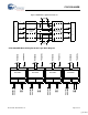
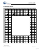
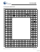
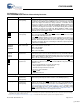
Pin Definitions
CYV15G0404RB Quad HOTLink II Deserializing Reclocker
Name IO Characteristics Signal Description
Receive Path Data and Status Signals
RXDA[9:0]
RXDB[9:0]
RXDC[9:0]
RXDD[9:0]
LVTTL Output,
synchronous to the
RXCLK± output
Parallel Data Output. RXDx[9:0] parallel data outputs change relative to the
receive interface clock. If RXCLKx± is a full-rate clock, the RXCLKx± clock outputs
are complementary clocks operating at the character rate. The RXDx[9:0] outputs
for the associated receive channels follow the rising edge of RXCLKx+ or the
falling edge of RXCLKx–. If RXCLKx± is a half-rate clock, the RXCLKx± clock
outputs are complementary clocks operating at half the character rate. The
RXDx[9:0] outputs for the associated receive channels follow both the falling and
rising edges of the associated RXCLKx± clock outputs.
When BIST is enabled on the receive channel, the RXDx[1:0] and BISTSTx
outputs present the BIST status. See Table 5, “Receive BIST Status Bits,” on
page 17 for each status that the BIST state machine reports. Also, while BIST is
enabled, ignore the RXDx[9:2] outputs.
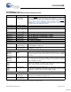
BISTSTA
BISTSTB
BISTSTC
BISTSTD
LVTTL Output,
synchronous to the
RXCLKx± output
BIST Status Output. When RXBISTx[1:0] = 10, BISTSTx (along with RXDx[1:0])
displays the status of the BIST reception. See Table 5, “Receive BIST Status Bits,”
on page 17 for the BIST status for each combination of BISTSTx and RXDx[1:0].
When RXBISTx[1:0] ≠ 10, ignore BISTSTx.
REPDOA
REPDOB
REPDOC
REPDOD
Asynchronous to
reclocker output
channel
enable / disable
Reclocker Powered Down Status Output. REPDOx asserts HIGH when the
associated channel’s reclocker output logic powers down. This occurs when
disabling ROE2x and ROE1x by setting ROE2x = 0 and ROE1x = 0.
Receive Path Clock Signals
TRGCLKA±
TRGCLKB±
TRGCLKC±
TRGCLKD±
Differential LVPECL or
single-ended
LVTTL input clock
CDR PLL Training Clock. The frequency detector (Range Controller) of the
associated receive PLL uses the TRGCLKx± clock inputs as the reference source
to reduce PLL acquisition time.
In the presence of valid serial data, the recovered clock output of the receive CDR
PLL (RXCLKx±) has no frequency or phase relationship with TRGCLKx±.
When a single-ended LVCMOS or LVTTL clock source drives the clock, connect
the clock source to either the true or complement TRGCLKx input, and leave the
alternate TRGCLKx input open (floating). When an LVPECL clock source drives
it, the clock must be a differential clock, using both inputs.
RXCLKA±
RXCLKB±
RXCLKC±
RXCLKD±
LVTTL Output Clock Receive Clock Output. RXCLKx± is the receive interface clock that controls
timing of the RXDx[9:0] parallel outputs. These true and complement clocks
control timing of data output transfers. These clocks output continuously at either
the half-character rate (1/20 the serial bit-rate) or character rate (1/10 the serial
bit-rate) of the data being received, as selected by RXRATEx.
RECLKOA
RECLKOB
RECLKOC
RECLKOD
LVTTL Output Reclocker Clock Output
. The associated reclocker output PLL synthesizes the
RECLKOx output clock, which operates synchronous to the internal recovered
character clock. RECLKOx operates at either the same frequency as RXCLKx±
(RXRATEx = 0), or at twice the frequency of RXCLKx± (RXRATEx = 1). The
reclocker clock outputs have no fixed phase relationship to RXCLKx±.
Device Control Signals
RESET
LVTTL Input,
asynchronous,
internal pull up
Asynchronous Device Reset. RESET initializes all state machines, counters,
and configuration latches in the device to a known state. RESET
must assert LOW
for a minimum pulse width. When the reset is removed, all state machines,
counters and configuration latches are at an initial state. According to the JTAG
specifications, the device RESET
cannot reset the JTAG controller. Therefore, the
JTAG controller has to be reset separately. Refer to “JTAG Support” on page 17
for the methods to reset the JTAG state machine. See Table 3, “Device Configu-
ration and Control Latch Descriptions,” on page 14 for the initialize values of the
device configuration latches.
[+] Feedback