CY24272 Rambus® XDR™ Clock Generator with Zero SDA Hold Time Features ■ Table 1. Device Comparison Meets Rambus® Extended Data Rate (XDR™) clocking requirements ■ 25 ps typical cycle-to-cycle jitter ❐ –135 dBc/Hz typical phase noise at 20 MHz offset ■ 100 or 133 MHz differential clock input ■ 300–667 MHz high speed clock support ■ Quad (open drain) differential output drivers ■ Supports frequency multipliers: 3, 4, 5, 6, 9/2 and 15/4 ■ Spread Aware™ ■ 2.
CY24272 Pinouts Figure 1. Pin Diagram - 28 Pin TSSOP VDDP VSSP ISET VSS REFCLK VDDC VSSC SCL SDA EN ID0 ID1 /BYPASS CY24272 REFCLKB 1 2 3 4 5 6 7 8 9 10 11 12 13 14 28 27 26 25 24 23 22 21 20 19 18 17 16 15 VDD CLK0 CLK0B VSS CLK1 CLK1B VDD VSS CLK2 CLK2B VSS CLK3 CLK3B VDD Table 2. Pin Definition - 28 Pin TSSOP Name IO 1 Pin No. VDDP PWR 2.
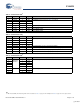
CY24272 PLL Multiplier Table 3 shows the frequency multipliers in the PLL, selectable by programming the SMBus registers MULT0, MULT1, and MULT2. Default multiplier at power up is 4. Table 3.
CY24272 Table 5.
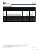
CY24272 Table 6. Command Code 80h[5] Bit Register POD Type Description 7 Reserved 0 RW Reserved (no internal function) 6 MULT2 0 RW PLL Multiplier Select (reference Table 3 on page 3) 5 MULT1 0 RW 4 MULT0 1 RW 3 RegA 1 RW Clock 0 Output Select 2 RegB 1 RW Clock 1 Output Select 1 RegC 1 RW Clock 2 Output Select 0 RegD 1 RW Clock 3 Output Select Table 7.
CY24272 Figure 2. Differential and Single-Ended Clock Inputs Supply Voltage V TH REFCLKB Input Input REFCLK REFCLK XDR Clock Generator XDR Clock Generator Differential Input Single-ended Input Absolute Maximum Conditions Parameter Description Condition Min Max Unit –0.5 4.6 V VDD Clock Buffer Supply Voltage VDDC Core Supply Voltage –0.5 4.6 V VDDP PLL Supply Voltage –0.5 4.6 V VIN Input Voltage (SCL and SDA) Relative to VSS –0.5 4.
CY24272 DC Operating Conditions Parameter Description Condition Min Max Unit 2.5V ± 5% 2.375 2.625 V VDDP Supply Voltage for PLL VDDC Supply Voltage for Core 2.5V ± 5% 2.375 2.625 V VDD Supply Voltage for Clock Buffers 2.5V ± 5% 2.375 2.625 V VIHCLK Input High Voltage, REFCLK/REFCLKB 0.6 0.95 V VILCLK Input Low Voltage, REFCLK/REFCLKB –0.15 +0.
CY24272 AC Operating Conditions The AC operating conditions follow.[6] Parameter tCYCLE,IN Description Condition REFCLK, REFCLKB input cycle time Min Max Unit REFSEL = 0, /BYPASS = High 9 11 ns REFSEL = 1, /BYPASS = High 7 8 ns /BYPASS = Low 4 – ns – 185 ps Over 10,000 cycles 40% 60% tCYCLE Measured at 20%–80% of input voltage for REFCLK and REFCLKB inputs 175 700 ps Rise and Fall Times Difference – 150 ps Modulation Index for triangular modulation – 0.
CY24272 AC Electrical Specification The AC Electrical specifications follow. [6] Parameter tCYCLE tJIT(cc) Description Min Clock Cycle time[19] Typ 1.25 [20] Max Unit 3.34 ns Jitter over 1-6 clock cycles at 400–635 MHz – 25 40 ps Jitter over 1-6 clock cycles at 638–667 MHz – 25 30 ps L20 Phase noise SSB spectral purity L(f) at 20 MHz offset: 400–500 MHz (In addition, device must not exceed L(f) = 10log[1+(50x106/f)2.
CY24272 Test and Measurement Setup Figure 3. Clock Outputs Measurement Point V TS R1 CLK Swing Current Control R2 R3 C VT R T1 Z CH R T2 S Differential Driver ISET Measurement Point V TS R RC R1 CLKB R2 Example External Resistor Values and Termination Voltages for a 50Ω Channel Parameter Value Unit R1 33.0 Ω R2 18.0 Ω R3 17.0 Ω RT1 60.4 Ω RT2 301 Ω CS 2700 pF RRC 432 Ω VTS 2.5V V VT 1.
CY24272 Figure 4. Input and Output Waveforms VH 80% V (t) 20% VL tR tF Figure 5. Crossing Point Voltage CLK Vx+ Vx.nom Vx- CLKB Figure 6. Cycle-to-cycle Jitter CLK CLKB tCYCLE,i tCYCLE,i+1 tJ = tCYCLE,i - tCYCLE,i+1 over 10,000 consecutive cycles Figure 7. Cycle-to-cycle Duty-cycle Error CLK CLKB tPW-(i) tCYCLE,(i) tPW+(i) tPW-(i+1) tPW+(i+1) tCYCLE,(i+1) tDC,ERR = tPW-(i) - tPW-(i+1) and tPW-(i+1) - tPW+(i+1) Document Number: 001-42414 Rev.
CY24272 Ordering Information Part Number Package Type Product Flow Pb-Free CY24272ZXC 28-pin TSSOP Commercial, 0°C to 70°C CY24272ZXCT 28-pin TSSOP – Tape and Reel Commercial, 0°C to 70°C Package Drawing and Dimension Figure 8. 28-Pin Thin Shrunk Small Outline Package (4.40-mm Body) ZZ28 PIN 1 ID 1 4.30[0.169] 4.50[0.177] 6.25[0.246] 6.50[0.256] 28 0.65[0.025] BSC. 0.19[0.007] 0.30[0.012] 1.10[0.043] MAX. 0.25[0.010] BSC GAUGE PLANE 0°-8° 0.076[0.003] 0.85[0.033] 0.95[0.037] 9.60[0.
CY24272 Document History Page Document Title: CY24272 Rambus® XDR™ Clock Generator with Zero SDA Hold Time Document Number: 001-42414 REV. ECN NO. Issue Date ** 1749003 See ECN Orig. of Change Description of Change KVM/AESA New data sheet No 8 or 15/2 multipliers or 133MHz * 4 option Max frequency is 667MHz © Cypress Semiconductor Corporation, 2007. The information contained herein is subject to change without notice.