
Clock Generator with Zero SDA Hold Time Specification Sheet


CY24272
Document Number: 001-42414 Rev. ** Page 10 of 13
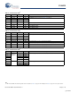
Test and Measurement Setup
Figure 3. Clock Outputs
Signal Waveforms
A physical signal that appears at the pins of a device is deemed
valid or invalid depending on its voltage and timing relations with
other signals. Input and output voltage waveforms are defined as
shown in Figure 4 on page 11. Both rise and fall times are defined
between the 20% and 80% points of the voltage swing, with the
swing defined as V
H
–V
L
.
Figure 5 on page 11 shows the definition of the output crossing
point. The nominal crossing point between the complementary
outputs is defined as the 50% point of the DC voltage levels.
There are two crossing points defined: Vx+ at the rising edge of
CLK and Vx– at the falling edge of CLK. For some waveforms,
both Vx+ and Vx– are below Vx,nom (for example, if t
CR
is larger
than t
CF
).
Jitter
This section defines the specifications that relate to timing uncer-
tainty (or jitter) of the input and output waveforms. Figure 6 on
page 11 shows the definition of cycle-to-cycle jitter with respect
to the falling edge of the CLK signal. Cycle-to-cycle jitter is the
difference between cycle times of adjacent cycles. Equal require-
ments apply rising edges of the CLK signal. Figure 7 on page 11
shows the definition of cycle-to-cycle duty cycle error (t
DC,ERR
).
Cycle-to-cycle duty cycle is defined as the difference between
t
PW+
(high times) of adjacent differential clock cycles. Equal
requirements apply to t
PW-
, low times of the differential click
cycles.
Differential Driver
CLK
CLKB
Swing Current
Control
ISET
R
RC
Measurement
Point
V
TS
R
1
Z
CH
V
T
R
T1
C
S
R
T2
R
3
R
2
Measurement
Point
V
TS
R
1
Z
CH
V
T
R
T1
C
S
R
T2
R
3
R
2
Notes
19. Max and min output clock cycle times are based on nominal outputs frequency of 300 and 667 MHz, respectively. For spread spectrum modulated differential or
single-ended REFCLK, the output clock tracks the modulation of the input.
20. Output short term jitter spec is the absolute value of the worst case deviation.
21. t
SKEW
is the timing difference between any two of the four differential clocks and is measured at common mode voltage. Δt
SKEW
is the change in t
SKEW
when the
operating temperature and supply voltage change.
22. t
CR,CF
applies only when appropriate R
RC
and output resistor network resistor values are selected to match pull up and pull down currents.
Example External Resistor Values
and Termination Voltages for a 50Ω Channel
Parameter Value Unit
R
1
33.0 Ω
R
2
18.0 Ω
R
3
17.0 Ω
R
T1
60.4 Ω
R
T2
301 Ω
C
S
2700 pF
R
RC
432 Ω
V
TS
2.5V V
V
T
1.2V V
[+] Feedback