
Clock Generator with Zero SDA Hold Time Specification Sheet


CY24272
Document Number: 001-42414 Rev. ** Page 5 of 13
Note
5. RW = Read and Write, RO = Read Only, POD = Power on default. See Table 3 on page 3 for PLL multipliers and Table 5 on page 4 for clock output selections.
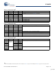
Table 6. Command Code 80h
[5]
Bit Register POD Type Description
7 Reserved 0 RW Reserved (no internal function)
6 MULT2 0 RW PLL Multiplier Select (reference Table 3 on page 3)
5MULT1 0 RW
4MULT0 1 RW
3 RegA 1 RW Clock 0 Output Select
2 RegB 1 RW Clock 1 Output Select
1 RegC 1 RW Clock 2 Output Select
0 RegD 1 RW Clock 3 Output Select
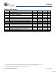
Table 7. Command Code 81h
[5]
Bit Register POD Type Description
7 Reserved 0 RW Reserved (no internal function)
6 Reserved 0 RW
5 Reserved 0 RW
4 Reserved 0 RW
3 Reserved 1 RW Reserved (must be set to ‘1’ for proper operation)
2 REFSEL 0 RW Reference Frequency Select (reference Table 3 on page 3)
1 Reserved 0 RW Reserved (must be set to ‘0’ for proper operation)
0 RegTest 0 RW Reserved (must be set to ‘0’ for proper operation)
Table 8. Command Code 82h
[5]
Bit Register POD Type Description
7Device
Revision
Number
? RO Contact factory for Device Revision Number information.
6?RO
5?RO
4?RO
3?RO
2 Vendor ID 0 RO Rambus assigned Vendor ID Code
11RO
00RO
[+] Feedback