
SoftStore nvSRAM Specification Sheet

STK11C68-5 (SMD5962-92324)
Document Number: 001-51001 Rev. *A Page 4 of 15
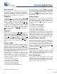
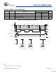
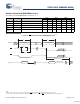
Low Average Active Power
CMOS technology provides the STK11C68-5 the benefit of
drawing significantly less current when it is cycled at times longer
than 50 ns. Figure 3 and Figure 4 shows the relationship
between I
CC
and Read or Write cycle time. Worst case current
consumption is shown for both CMOS and TTL input levels
(commercial temperature range, VCC = 5.5V, 100% duty cycle
on chip enable). Only standby current is drawn when the chip is
disabled. The overall average current drawn by the STK11C68-5
depends on the following items:
■ Duty cycle of chip enable
■ Overall cycle rate for accesses
■ Ratio of Reads to Writes
■ CMOS versus TTL input levels
■ Operating temperature
■ V
CC
level
■ I/O loading
Best Practices
Cypress nvSRAM products have been used effectively for over
15 years. While ease of use is one of the product’s main system
values, the experience gained from working with hundreds of
applications has resulted in the following suggestions as best
practices:
■ The nonvolatile cells in an nvSRAM are programmed on the
test floor during final test and quality assurance. Incoming
inspection routines at customer or contract manufacturer’s
sites sometimes reprograms these values. Final NV patterns
are typically repeating patterns of AA, 55, 00, FF, A5, or 5A.
The end product’s firmware must not assume that an NV array
is in a set programmed state. Routines that check memory
content values to determine first time system configuration.
■ Cold or warm boot status, and so on must always program a
unique NV pattern (for example, complex 4-byte pattern of 46
E6 49 53 hex or more random bytes) as part of the final system
manufacturing test. This is to ensure these system routines
work consistently.
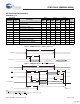
Figure 3. Current Versus Cycle Time (Read)
Figure 4. Current Versus Cycle Time (Write)
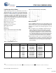
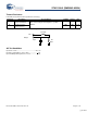
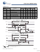
Table 1. Hardware Mode Selection
CE WE A12–A0 Mode I/O Notes
L H 0x0000
0x1555
0x0AAA
0x1FFF
0x10F0
0x0F0F
Read SRAM
Read SRAM
Read SRAM
Read SRAM
Read SRAM
Nonvolatile STORE
Output Data
Output Data
Output Data
Output Data
Output Data
Output High Z
[1]
L H 0x0000
0x1555
0x0AAA
0x1FFF
0x10F0
0x0F0E
Read SRAM
Read SRAM
Read SRAM
Read SRAM
Read SRAM
Nonvolatile RECALL
Output Data
Output Data
Output Data
Output Data
Output Data
Output High Z
[1]
Note
1. The six consecutive addresses must be in the order listed. WE
must be high during all six consecutive CE controlled cycles to enable a nonvolatile cycle.
[+] Feedback