
USB and Mass Storage Peripheral Specification Sheet

Schematic Review Checklist for
West Bridge
®
Astoria™
December 12, 2008 Document No. 001-46860 Rev. *A 1
AN46860
Author: Praveen Kumar
Associated Project: No
Software Version: Astoria SDK 1.0
Associated Application Notes: None
Application Note Abstract
West Bridge
®
Astoria™ is a USB and mass storage peripheral control device that contains three main ports: processor
interface (P-port), mass storage support (S-port), and USB interface (U-port). This application note discusses the hardware
recommendations and guidelines to design a system using Astoria.
Introduction
The West Bridge
®
Astoria™ device is a peripheral controller
that supports high speed USB and mass storage access.
This controller provides access from a processor interface
and a high speed USB (HS-USB) interface to peripherals
including SD, MMC/MMC+, CE-ATA, SDIO, SLC, and MLC
NAND. It supports interleaving accesses between the
processor interface, HS-USB, and peripherals. This enables
an external processor and an external USB host to transfer
data simultaneously to each other and to the mass storage
peripherals.
The hardware considerations to design Astoria into a system
are:
P-Port
1. If operating in the asynchronous mode, CLK is tied
LOW through a 10k resistor. In the synchronous mode,
CLK is connected to the incoming signal from the
processor interface.
2. In PCRAM and ADM mode, ADV# is tied to a signal on
the processor interface that conforms to the timing
specified in the West Bridge: Antioch USB/Mass
Storage Peripheral Controller data sheet. If the signal is
not available, tie ADV# to the CE# signal of the
processor interface.
3. The DRQ Status Register and DRQ Mask Register
indicate the available endpoints for transfer. They must
be accessed even if a DMA or burst operation is not
being implemented on the P-port interface. Use the
DRQ# or the INT# signal to indicate to the processor
that at least one of the bits in the DRQ Status Register
is set. If INT# is used, an extra read of the P-port
Interrupt Register must be done before the DRQ Status
Register is read. In PNAND mode, R/B is used as an
indication of End Point availability and is treated
differently in LNA and nonLNA modes.
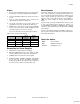
4. Ensure that TEST[2:0], A7, A3, and A2 settings are
correct for the various P-port interface configurations.
Table 1 lists the TEST[2:0] and register settings for
P-port interface configurations.
Table 1. P-Port Interface Configuration Options
TEST
[2:0]
VMTYPE Field in
CY_AN_MEM_P0_VM_S
ET Register
Interface
000
101
Non ADM PCRAM
000
111
SRAM
010
X
Extended Interface Mode
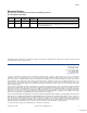
Table 2 lists the TEST[2:0] and address pin settings for
the various extended interface modes.
Table 2. Extended Interface Modes
TEST
[2:0]
A7
A3
A2
Interface
010
1
0
0
PNAND Mode-Small Block Device
010
0
0
0
PNAND Mode-Large Block Device
010
1
0
1
Address/Data Bus Multiplexing
(ADM)
010
1
1
0
SPI Mode
5. When using extended P-port modes, SCL and SDA (A5
and A6) require external pull up. The pull up resistors
are determined by the supply voltage, clock speed, and
bus capacitance. A typical value for the I2C pull ups is
2 kΩ. This value must be adjusted based on the trace
length and board layout conditions. The pull up on SDA
is required even if I
2
C™ EEPROM is not being used. A
low value resistor can cause overshoot and a high
value resistor can cause timing violation depending on
the capacitance on the bus.
[+] Feedback