
USB and Mass Storage Peripheral Specification Sheet

AN46860
December 12, 2008 Document No. 001-46860 Rev. *A 2
6. DACK# is used in conjunction with DRQ#. If INT# is
used to indicate that at least one bit is set in the DRQ#
register, then DACK# remains unused. DACK# is not
required for Astoria to function.
7. INT#, DRQ#, and DACK# are in GVVDQ power
domain. Therefore, pull up the input pin DACK# to
GVDDQ using a 10k resistor, if it is not used.
8. All unused inputs and input or output pins on the P-port
are tied to a valid logic level (HIGH for lowest leakage)
through a 10k resistor. Use a single resistor for all
unused pins. When pulling HIGH, the unused pins are
tied to the appropriate power domain, in this case,
PVDDQ or GVDDQ.
Refer to the Pin Assignments table in the data sheet for
more details on pin configuration for each P-port
interface mode and their corresponding power domains.
9. The INT# and DRQ# signals float when Astoria is in
Standby state. These signals are active low. As a result,
a pull up resistor must be connected to these signals to
prevent the P-port processor from receiving any false
interrupts.
10. In the PNAND Interface Mode, external pull up is not
required for the R/B# signal. R/B# signal is not an open
drain or collector output.
S-Port
1. Use SD_D[3]/SD2_D[3] or GPIO[0]/GPIO[1] to detect
cards on Astoria. If SD_D[3]/SD2_D[3] is used, then it
must be pulled down using a 470 kΩ resistor.
2. Treat the SD_CLK signal as a high speed signal
switching at a maximum of 48 MHz to determine the
appropriate signal integrity precautions.
3. If you are designing an application supporting SD/MMC
and CE-ATA, follow the trace length restrictions.
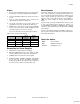
Table 3 lists acceptable frequencies for Astoria, and the
maximum trace lengths corresponding to the
frequencies for SD cards that cannot operate in high
speed mode.
Table 3. Frequency vs. Trace Length (SD Default Mode)
SDFREQ (MHz)
Maximum Trace Length (in)
24.00
1.94
21.82
7.55
20.00
13.17
18.46
18.78
17.14
24.4
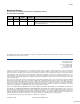
Table 4 lists the acceptable frequencies for Astoria and
the corresponding maximum trace lengths for SD cards
that are capable of operating in high speed mode.
Table 4. Frequency vs. Trace Length (SD High Speed
Mode)
SDFREQ (MHz)
Maximum Trace Length (in)
48.00
8.18
40.00
20.66
34.29
33.13
30.00
45.61
26.67
58.08
Refer to the Pin Assignments table in the data sheet for
more details on pin configuration for each pin in each
S-port configuration and their corresponding power
domains.
4. All unused inputs and input or output pins on the S-port
are tied to a valid logic level (HIGH for lowest leakage)
through a 10k resistor. Use a single resistor for all
unused pins. When pulling HIGH, the unused pins are
tied to the appropriate power domain, in this case,
SSVDDQ, SNVDDQ, or GVDDQ.
5. The pull up resistor (Rp) used for NAND_R/B# varies
from 1k to 10k based on the timing requirements and
the manufacturer of the NAND device.
6. The SD_POW signal floats when Astoria is in standby.
If this signal is used to control power to the SD card
through an external switch, a pull up or pull down
resistor must be connected on SD_POW, such that the
switch remains ON and power to the card is retained
during Astoria’s standby condition.
U-Port
1. To avoid an impedance mismatch, lay out the USB
differential signals (D+ and D-) with constant spacing
and on one plane. Avoid vias and stubs. It is prudent to
lay out the signals before laying out the rest of the
board.
2. Minimize the trace lengths between the D+ and D- pins
on Astoria and the USB connector.
3. If unused, SWD+/SWD– lines must be left floating or
pulled low. A high on these lines may cause the USB to
overlook detection in the system.
For further information, refer to the Cypress Application Note
AN1168, High Speed USB PCB Layout Recommendations.
[+] Feedback