DVD PLAYER DVG-4000N SERVICE MANUAL
CONTENTS 1.
1. Precautions 1-1 Safety Precautions 1) Before returning an instrument to the customer, always make a safety check of the entire instrument, including, but not limited to, the following items: (1) Be sure that no built-in protective devices are defective or have been defeated during servicing. (1) Protective shields are provided to protect both the technician and the customer. Correctly replace all missing protective shields, including any remove for servicing convenience.
notes non or inside the cabinet, or on the chassis. 3) Design Alteration Warning-Do not alter of add to the mechanical or electrical design of this instrument. Design alterations and additions, including but not limited to, circuit modifications and the addition of items such as auxiliary audio output connections, might alter the safety characteristics of this instrument and create a hazard to the user.
components, and wiring have been installed correctly and that the portion around the serviced part has not been damaged and so on. Further, check the insulation between the blades of the attachment plus and accessible conductive parts. 1-2-2 Insulation Checking Procedure turn the power ON. Connect the insulation resistance meter (500V) to the blades of the attachment plug.
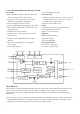
2. Reference Information 2-1 Component Descriptions 2-1-1 DVD ATAPI Loader D.C. Power Supply A 4-pin shrouded, keyed male connector is used to provide the D.C.Power. The pin assignment is described below. PIN 1 2 3 4 DC VOLTS +12V GND GND +5V Interface Connector A 39-pin male, unshielded, shrouded, keyed connector are applied. Please refer to Section 7-2-3 regarding its pin definition. Electrical Characteristics 1. Power 1-1. Voltage +5V DC with ± 5% tolerance.
I/F Signals I/O Pin # I/F Signals I/O Pin # DD12 12 IOCS16 32 DD2 13 DA1 33 DD13 14 PDIAG 34 DD1 15 DA0 35 DD14 16 DA1 36 DD0 17 CS1FS 37 DD15 18 CS3FS 38 GND 19 DASP 39 NC 20 GND 40 4.
2-1-2 NTSC/PAL Digital Video Encoder (AV3168) FEATURES • Fully CCIR 624 performance compliance NTSC and PAL (B,D,G,H,I,M and N) video encoder. • Composite, S-video, Component Y/Cb/Cr (Sony, Matsushita, and SMPTE) or RGB output. • Triple 10-bit digital to analog converter. • Accepts 27 Mhz multiplexed 8-bit digital video inputs. • Master or Slave 4-Field NTSC or 8-Field PAL video timing generation. • CCIR 656 EAV SYNC extraction. • Automatic NTSC or PAL timing detection in slave mode operation.
The Clock Generator outputs three clocks for video, audio and system to simplify the system configuration and maintain A/V synchronization.
PIN DESCRIPTIONS Pin Name Pin # Type Description DIGITAL VIDEO INPUT PD<7 -0> 11-16 18-19 I HSYN 20 I/O VSYN 21 I/O Multiplexed Cb, Y, and Cr digital video input bus. In Slave Mode (MSTR pin is low) Horizontal Synch input. In Master Mode (MSTR pin is high) Horizontal Synch output. In slave mode (MSTR pin is low) Vertical Sync input. In master mode Vertical Sync output.
Pin Name Pin # Type Y 31 O C 33 O VREF 40 I/O IREF 39 I COMP 38 I BIAS 37 I/O Description 1 X 0: Cr output in CbCr component mode 1 0 X: : 1 1 1: Blue color output in RGB mode Analog video output Determined by the state of CPNT pin and CR0[5:4] CPNT CR0[5] CR0 [4] 0 X X: S-Video Y output. 1 X 0: Cb output in CbCr component mode 1 0 X: : 1 1 1: R color output in RGB mode Analog video output Determined by the state of CPNT pin and CR0[5:4] CPNT CR0[5] CR0 [4] 0 X X: S-Video C output.
Pin Name Pin # Type Description GCK frequency select pin when RST is low. General purpose output pin when RST is high Dual function pin. GOUT0 43 I GCK frequency select pin when pin when RST is low.
* Functional Description 11
* Pinout Diagram 12
* PIN DESCRIPTON Name Number I/O Definition I 3.65 V ± 150 mv. O Device address output I Ground I O 71 74:72 96:93, 90:85, 82:77 97,100 101 102 105 115:113, 110:106 I/O I/O O I I I I I O O O O I O O I/O O O O I O Reset input active low. TDM transmit data ROM Select RSEL Selection 0 16-bit ROM 1 8-bit ROM TDM receive data. TDM clock input. TDM frame synch. TDM output enable, active low. Audio transmit frame sync. Select PLL1. Audio transmit serial data port. Select PLL0.
Name Number I/O Definition HD[15:0] HCS1FX# HCS3FX# HIOCS16# HA[2:0] VPP HWR#/DCI_ ACK# HRD#DCI-C LK HD[15:0] HWRQ# HRDQ# HIRQ HRST# HIORDY HWR# AUX[7:0] LOE# LCS[3:0]# LD[15;0] LWRLL# LWRHL# NC 141:140, 137:131, 128:122 152 153 151 158, 155:154 159 O O O I I/O I 149 I,I 150 I,I Host read/DCI Interface Clock. 141:140, 137:131, 128:122 142 143 144 145 146 149 169:165, 162:160 170 176:173 197:194, 191:185, 182:178 198 199 37, 38, 42, 203:202 I/O O O I/O O I O I/O O O I/O O O Host data bus.
PIN DESCRIPTIONS 2-1-5 Serial EEPROM, 2K (256 x 8) (AT24C02/01) * Features Low-Voltage and Standard-Voltage Operation -5.0 (V CC = 4.5V to 5.5V) -2.7 (V CC = 2.7V to 5.5V) -2.5 (V CC = 2.5V to 5.5V) -1.8 (V CC = 1.8V to 5.
Internally Organized 128 x 8 (1K), 256 x 8 (2K), 512 x 8 (4K), 1024 x 8 (8K) or 2048 x 8 (16K) 2-Wire Serial Interface Schmitt Trigger, Filtered Inputs for Noise Suppression Bi-directional Data Transfer Protocol 100 kHz (1.8v, 2.5V, 2.
Integrated Product Identification Code Commercial and Industrial Temperature Ranges * Pin Configurations * Pin Description Pin Name A0 – A18 O0 – O7 CE# OE# Function Addresses Outputs Chip Enable Output Enable * Absolute Maximum Ratings Temperature Under Bias………………………….-55oC to + 125 oC Storage Temperature……………………………...-65 oC to + 150 oC Voltage on Any Pin with Respect to Ground……..-2.0V to + 7.0V Voltage on A9 with Respect to Ground…………...-2.0V to + 14.0V V PP Supply Voltage with Respect to Ground…….-2.
All inputs are sampled at the positive going edge of the system clock Burst Read Single-bit Write operation DQM for masking Auto & self refresh 64ms refresh period (4K cycle) 50 Pin TSOP (II) Pin Configuration 18
Block Diagram Pin Descriptions Symbol Name CLk System Clock CS Chip Select Description Active on the positive going edge to sample all inputs Disables or Enables device operation by masking or enabling all inputs except CLK, CKE and L(U)DQM Masks system clock to freeze operation from the next clock cycle.
Symbol Name L(U)DQM Data Input/Output Mask DW0-15 Data Input/Output VDD/VSS VDDQ/VSSQ Power Supply/Ground Data Output Power/Ground NC/RFU No Connection 20 Description Makes data output Hi-Z, t SHZ after the clock and masks the output. Blocks data input when L(U)DQM active. Data inputs/outputs are multiplexed on the same pins. Power Supply: +3.3V±0.3V/Ground Provide isolated Power/Ground to DQs for improved noise immunity.
3. Product Specifications Playback System DVD Video Video CD (1.1, 2.0, 3.0) SVCD and CVD CDDA CD-ROM with MP3 data Television Signal System NTSC/PAL Video Performance Video Out 1 Vpp into 75 ohm S-Video Out Y: 1Vpp into 75 ohm C: 0.286 Vpp into 75 ohm Component Out 0.7 Vpp into 75 ohm D/A Converter 27MHz/10bit Audio Performance Frequency Response DVD: fs 48/96KHz, 4Hz~22/44KHz Video CD: fs 44.1KHz, 4Hz~20KHz Audio CD: fs 44.1KHz, 4Hz~20KHz Output Level Analog: 2Vrms(1KHZ) Digital: 1.
4. Operating Instructions 4-1 Basic Connections * CONNECTED TO A TV * CONNECTED TO AN ORDINARY AMPLIFIER R L 4-2 Selecting Video MODE Press SETUP button and select GENERAL SETUP submenu on SETUP screen. After that, select TV TYPE by pressing DOWN arrow button (▼ ) until desired TV mode is selected. For more information, refer to Page 34-36 on the Instruction Manual.
4-3 Selecting the desired DVD menu Item Some DVDs have title menus and chapter menus. Press MENU or TITLE,the screen shows the menu.Then use direction buttons to select the desired item,press PLAY. 4-4 Selecting the desired MP3 folder Use arrow button to select the folder you want to play. Then by pressing the PLAY button ,you can see the the file lists under the folder.
4-8 Slow Viewing When you want to view the disc contents very slowly in forward or reverse direction, you can do that by pressing the SLOW button. When playing DVD,there are six choices:SF2X, SF4X, SF8X, SR2X, SR4X, SR8X. While playing SUPER-VCD OR VCD,there are three choices: SF1x, SF2x, SF3x.Take DVD for example, to view at slow 2x in reverse direction ,press the slow buttom four times. To resume playing normally ,just press PLAY.
5.
6. Troubleshooting No power No picture No sound Distorted sound Insert the AC power plug securely into the power outlet. Make sure that the equipment is connected properly. Make sure that the input setting for TV is Video (AV). Make sure that the equipment is connected properly. Make sure that the input settings for the TV and stereo system are correct. No fast forward or fast reverse Some discs may have sections that prohibit fast forward or fast reverse.
7. Electrical Part List DVG-4000N PRODUCT DESIGN PACKAGE LIST No. Name Counts Blueprint No. Material No. Notes 1 DVG4000N surface subassembly 1 BC-PMGDVG3000N 2 HPT DVD machine core 1 JX-HPTAM-2266 3 bracket of machine core 2 WJ-JXZJ930E5 the height of HPT machine core:17.
No. Counts Blueprint No. Material No.
No. Name Counts Blueprint No. Material No.
No. Name Counts 45 2.54 connector/2.54connctor 6P red-white row-wire 260mm 1 Blueprint No. Material No. Notes from power-supply board PX-B260B6R board to The list for cover subassembly design of DVG4000N No. 30 Name Counts Blueprint No. Material No.
No. Name Counts Blueprint No. Material No. 16 plain-headed triangular nail BB3*8 colorful zinc 16 LD-BB3*8C 17 power-supply cover 1 SJ-DYG 18 safety pasting-paper 1 FL-ACTZ 19 ordinary green round-headed LED 1 FG-3MMBFLGL Notes control panel 9 bracket for cover 4 microphone board 1 power-supply switch 2 diameter: 3mm round-headed The components design list for control panel No. Name/Specification Counts Position in the paper Material No.
No. Name/Specification Counts Position in the paper Material No.
The component design list for DV-910 earphone board No. Name Counts resistor resistor 10E 1/4W 1 10% 2 resistor 1K 1/4W 10% resistor 4.7K 1/4W 3 10% resistor 5.1K 1/4W 4 10% 5 100K 1/4W 10% resistor 22K 1/4W 6 10% resistor 47K 1/4W 7 10% porcelain capacitor porcelain capacitor 101 8 50V 10% electrolyzed capacitor 9 electrolyzed 16V 20% capacitor 10UF 10 electrolyzed capacitor 100UF 16V 20% Blueprint No. Material No.
No. Name changeable 14 R1216G11A2-A20K mode 15 PCB GV-DHB910 16 jumper Counts resistor six-foot 10mm 2 Blueprint No. RW1,RW2 1 3 J1,J2,J3 Material No. Notes DW-WT1Z20KS01 PCBDHB910 2001.04.28 FJ-TX10MM diameter:0.6mm 17 bracket for microphone board round-headed self-fastened 18 hardened nail BTV3*6 colorful zinc 1 WJMBZJ320 1 LDBBTV3*6C.
8.
9. Circuit Diagrams 1. Control Part 2. Ear Part 3. Video Part 4. Clock Part 5. Memory Part 6. Chip 4318 7. D/A Converter Part 8. Atapi Part 9. Audio Part 10.
1 2 3 4 5 6 D D IC1 HT6221 1 2 3 4 5 6 7 8 9 10 C2 C1 100u/16V 104 L1 LED X1 455E CZ2 1 2 3 4 5 6 +5V IR GND CLK CS DATA VCC SIG GND C3 271 Q1 9014 K10 KEY K6 KEY K5 KEY K11 KEY K14 KEY K9 KEY K8 KEY K7 KEY K13 KEY K12 KEY K22 KEY K21 KEY C4 271 K17 KEY R2 47E 6PIN C 20 19 18 17 16 15 14 13 12 11 3 2 1 C K4 KEY K3 KEY K16 KEY K15 KEY K24 KEY K19 KEY K2 KEY K1 KEY K18 KEY K20 KEY K25 KEY K23 KEY +5V REMOTE REM CZ3 1 +4.
2 3 C7 10uF R4 4.7K 4 4 1 IC1A UJM4558 2 C2 10uF 1 R2 10E 3 D D C4 100pF 8 1/2VCC VCC VCC C18 10uF XH1 C 4 3 2 1 VCC 4P2D54 R19 22K R21 1K 7 1/2VCC R1 10E 6 C6 10uF C3 100pF C16 10uF R24 5.1K R18 100K C1 10uF 5 R6 4.7K Q2 C1815 R20 22K MIC1 CK-6.35-305 IC1B UJM4558 R16 5.1K VCC +12V GND Rin Lin R5 47K RW1 RD902G-BA1-A20K R17 100K C R3 47K R18 5.1K C13 10uF R12 4.7K IC2B UJM4558 5 MIC2 CK-6.35-305 C10 10uF 7 R9 10E 6 C17 10uF R22 1K +12V R23 5.
1 2 3 VVCC 4 TVCC FB5 FERRITE BEAD +5V VVCC FB1 FERRITE BEAD + C73 47uF D C60 0.1uF C70 0.1uF D + C89 100uF C68 0.1uF C65 22pF L2 4.7uH C67 10pF C66 22pF XH1 27.0000MHz R106 100k TVCC C61 22pF SW1D AV6 CR/B VVCC 6 5 4 3 2 1 44 43 42 41 40 R92 200 Q1 9014 1K(open) 7 8 9 10 11 12 13 14 15 16 17 U9 AV3168/9 D6 IN4148 C58 180pF C62 180pF C54 IREF COMP BIAS VDDA CVBS VSS C VDDA Y VSS VDDA 39 38 37 36 35 34 33 32 31 30 29 C 0.1uF TVCC C56 C63 22pF 0.
1 2 R151 3 (OPEN) 4 VCC C145 10U/16V R169 330E R168 10K D R150 0 OHM R59 27M D RST# Q5 JE9014 33 OHM DCLK D7 1N4148 R170 10K OPEN E2 C22 OPEN LFA30-2A1E473MB U16 1 2 3 4 5 (15PF) VCC 33 OHM R64 NC GND NC RES VDD XIN V6300 Package: SOT-23 5L No need if using CAT24C021 C24 OPEN E4 LFA30-2A1E473MB (15PF) VCC C C R63 R137 4.
1 DMA[0..
1 2 3 VCC3 4 VCC Install R100 for ES4308 TDMDX RST# LCS0# LCS1# LCS2# LCS3# LCS2# 198 199 WRLL# WRHL# 170 LOE# LA[0..19] LA0 LA1 LA2 LA3 LA4 LA5 LA6 VCC LA7 LA8 TWS LA9 LA10 LA11 4.7K LA12 LA13 R50 C LA14 TDMDX LA15 LA16 LA17 4.7K LA18 LA19 LD[0..7] LD0 LD1 LD2 LD3 LD4 LD5 LD6 LD7 LD[8..
1 2 3 4 D D VA CS4338 7 VCCA1 U18 AOUTL 8 R200 10 VCCA1 C137 0.
1 2 R1 3 DRST# HRST# 4 JS3 47 OHM DWR# DD15 DD14 47 OHM VCC VCC DD13 DD12 R21 DRD# HRD# DD11 DD10 47 OHM D R22 R24 4.7K R23 4.
1 2 3 4 +12V R196 10E JS2 1 2 3 4 +12VA D C165 C168 10U/25V 100U/25V MIC D 4PIN 2.54 R198 10K C169 100U/16V JS6 1 2 3 4 1/2VCC R197 10K L OUT R OUT FB2 FB +12VA 4PIN 2.54 C C 18K C156 150P 12V R201 15K R189 22K OPEN +12VA LIN R172 100k R178 22K 8 R175 3.3K 3 + 2 - C162 1000P U23A C158 4.7U/16V 1 R185 100K C160 22P R187 SW1B AV6 L OUT 3 MPOP-14 OPEN R188 ZR0 R203 10K 10K OPEN R183 1K Q7 A1015 OPEN Q8 2SC1815 OPEN Q4 2SC1815 0E R204 OPEN 10K 2 C151 R176 4.
1 2 3 4 D 5 6 D ! ! CON1 L 1 2 3 4 1 2 3 4 ! T2AL 250V F1 1 ! 10E 2A D7 HER302 AABB 17 C1 2K2 2W C2 C13 D2 4 1N4005 D3 1N4005 56T C8 C9 47P 1KV 68UF 400V 10E 1/4W R7 R17 1000UF 16V R8 2K2 2K2 1/4W C15 1K 30P 1KV 222 400V C16 6T 6 18,15 C7 222PF 400V C5 ! C6 ! 3300PF 400V 3300PF 400V 14 ! C R10 OR Open Pin1 C17 D9 C19 R11 OR Open Pin2 M4 UF4004 470UF 10V 2K 1/8W 1000UF10V 14T M1 TOP223 D6 13 UF4004 26T 1 ! D10 C20 D11 C23 100UF 50V
10.