Service Manual XGA COLOR MONITOR Model : L510B1 DAEWOO ELECTRONICS CO., LTD. http : //svc.dwe.co.
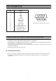
CONTENTS SAFETY PRECAUTIONS 1 GENERAL SAFETY INFORMATION 2 SERVICING PRECAUTIONS 3 TECHNICAL INFORMATION 6 GENERAL INFORMATION 7 PIN CONNECTOR 8 CAUTIONS FOR ADJUSTMENT AND REPAIR 8 OPERATION & ADJUSTMENT 9 ALIGNMENT PROCEDURE 14 TROUBLESHOOTING HINTS 15 BLOCK DIAGRAM 22 PCB LAYOUT 23 SCHEMATIC DIAGRAM 27 EXPLODED VIEW & MECHANICAL PARTS LIST 29 INFORMATION OF PART DESCRIPTION 30 ELECTRICAL PARTS LIST 31
SAFETY PRECAUTIONS CAUTION: No modifications of any circuits should be attempted. Service work should be performed only after you are thoroughly familiar with all of the following safety checks and servicing guidelines. ◆ Safety Check Care should be taken while servicing the inverter that generates the high voltage to lighten CCFL of the LCD panel. ◆ Fire & Shock Hazard • Insert an isolation transformer between the analog color display and AC power line before servicing the chassis.
GENERAL SAFETY INFORMATION ◆ Terms in the manual CAUTION Statements identify conditions or practices that could result in damage to the equipment or other property. WARNING Statements identify conditions or practices that could result in personal injury or loss of life. ◆ Terms as marked on equipment CAUTION Statements indicate a personal injury hazard not immediately accessible as one reads the marking or a hazard which is properly included on the equipment itself.
SERVICING PRECAUTIONS CAUTION: Before servicing instruments covered by this service manual, its supplements, and addendum, please read and follow the SAFETY PRECAUTIONS of this manual. NOTE: If unforeseen circumstances create conflict between the following servicing precautions and any of the safety precautions on page 1 of this manual, always follow the safety precautions. Remember: Safety First. ◆ General Servicing Precautions 1. Always unplug the AC power cord from the AC power source before: a.
◆ Electrostatically Sensitive (ES) Devices Some semiconductor (solid state) devices can be damaged easily by static electricity. Such components are commonly called Electrostatically Sensitive (ES) Devices. The typical examples of ES devices are integrated circuits, some field-effect transistors, and semiconductor “chip” components. The following techniques should be used to help reduce the incidence of component damage caused by static electricity. 1.
FIGURE 1. USE SOLDERING IRON TO PRY LEADS ◆ IC Removal/Replacement Some utilized chassis circuit boards have slotted (oblong) holes through which the IC leads are inserted and then bent flat against the circuit foil. When holes are slotted, the following technique should be used to remove and replace the IC. When working with boards using the familiar round hole, use the standard technique as outlined in paragraphs 5 on the page under the title of general soldering guidelines. ◆ Removal 1.
◆ Diode Removal/Replacement 1. Remove defective diode by clipping its leads as close as possible to diode body. 2. Bend the two remaining leads perpendicularly to the circuit board. 3. Observing diode polarity, wrap each lead out of the new diode around the corresponding lead on the circuit board. 4. Securely crimp each connection and solder it. 5. Inspect the solder joints of the two “original” leads on the circuit board copper side.
GENERAL INFORMATION This TFT LCD monitor automatically scans all horizontal frequencies from 30KHz to 62KHz, and all vertical frequencies from 50Hz to 75Hz. This TFT LCD monitor supports IBM PC, PC/XT, PC/AT, personal System/2 (PS/2), Apple Macintosh, and compatible users crisp text and vivid color graphics display when using the following graphics adapters : (VGA, Super VGA, VESA and XGA and Apple Macintosh Video Card).
PIN CONNECTOR Pin Signal 1 2 3 4 5 6 7 8 9 10 11 12 13 14 15 Red Green Blue GND GND GND - Red GND - Green GND - Blue +5Vdc GND - H.Sync GND - V.Sync Bi-directional Data (SDA) Horizontal Sync Vertical Sync (VCLK) Data Clock (SCL) 1 6 10 15 Arrangement of 15-pin D-sub connector CAUTIONS FOR ADJUSTMENT AND REPAIR • Degaussing is always required when adjusting purity or convergence. • The white balance adjustment has been done by a color analyzer in factroy.
OPERATION AND ADJUSTMENT Control Panel AUTO AUTO EXIT MENU BRIGHTNESS BRIGHTNESS EXIT MENU BRIGHTNESS • The AUTO button launches the AUTO TRACKING function directly. • • The EXIT button turns the OSD (On-Screen Display) window off. • • The MENU button turns the OSD window on. • • The button moves cursor to the left or high window in the OSD window. • • The button moves cursor to the right or low window in the OSD window. This button moves from sub menu to top menu in the OSD window.
Key Process MENU UT L TY M E NU U T L TY OSD OSD MENU UT L T Y EXIT MENU SHARPNESS EXIT OSD OFF 10 EXIT SHARPNESS
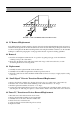
Adjustment Procedure No Is the H.Size proper? Adjust the CLOCK control. Yes Is the noise displayed on the screen? Perform the AUTO POSITION. No Yes Perform the AUTO TRACKING. Is the noise displayed on the screen yet? No Yes Adjust the CLOCK FINE until the screen is cleared.
OSD Functions ICON CONTROL FUNCTIONS LANGUAGE Select language for OSD (6 languages). CLOCK Adjust the width (horizontal size) of the screen image. CLOCK FINE Sharpen the focus by aligning the illuminated pixels and adjust until the screen image looks focused, crisp and sharp. Adjusting the CLOCK FINE after the CLOCK adjustment will produce a clear screen. AUTO TRACKING Adjust the horizontal & vertical picture image quality and size.
Self Diagnosis When the monitor doesn’t display, if you press any key, Self Diagnosis screen is displayed. Self Diagnosis function checks if the status of the monitor is No Signal or Out of range. No Signal screen is displayed when the D-Sub signal connector is not connected or the status of the monitor is on DPMS mode. Out of Range screen is displayed when the applied frequency is under or over normal range.
ALIGNMENT PROCEDURE Standard Check point 1. Power source : 100 - 240Vac, 50/60Hz. 2. Aging : Take at least 20 minutes warm-up time. 3. Signal Video input : Analog 0.7Vpp 75Ω terminal positive polarity Synchronizing : acceptable negative or positive at TTL level Max. Resolution : 1024 x 768 a 75Hz Frequency Horizontal : 30KHz - 62KHz Vertical : 50Hz - 75Hz (available only non interlace mode) Adjustment 1. Smart scaling set to 69%. 2. Contrast set to 90% 3. Brightness set to 50% 4.
TROUBLESHOOTING HINTS 1. Abnormal mode detect Abnormal mode detect Yes Is a input H-sync of ADC(pin 90, U2) correct? No Trouble in the H-sync input circuit. No Trouble in ADC. Yes Is waveform of pin 81 of ADC(U2) correct? Yes Trouble in Scaler(U1).
2. Trouble in Power on Is the Power LED toggled between on and off? On Refer to No video or No raster. Off Is the power cord well connected? No Check if the power switch is on position and Connect the power cord correctly. Yes Check the waveform of pin 7 of -com. No Trouble in U6 & Q5 and its ambient circuit. No Check the power board (5VS of CN2A). Yes Is 5VS line normal(pin 8 of CN2)? Yes Check on Scaler(U1).
3. No Raster Check the output of Q2 or pin 3 of U3. < 2.5 Trouble in Q6 or pin 3 of -com. > 2.5 Is 12V plugged in pin 1 of CN4A(power board)? No Check the output of D811(power board). Yes Is the output of inverter correct? No Yes Replace a LCD panal. 17 Replace the inverter.
4. One color is missing One color is missing Yes No Is the OSD color normal? Check the output signal of Scaler. Yes Is the input signal normal? No Check the video signal cable or R,G,B con-ass’y. Yes Are the R,G,B Digital values (every eight bits) correct on ADC output stage? Yes Trouble in the soldering of R,G,B data lines from output of ADC to Scaler(U1). 18 No Check the ambient circuit of ADC.
5. No Video Has display image only white? No Next page. Yes Check if the CN5 wafer is well connected at the LCD panel. No Connection trouble. Yes Is pin 1 of Q6 3.3V? No Yes Check the output of scalier (pin 71, 72, 73, 74, 75) and soldering of CN5. 19 Check Q6, its ambient circuit and pin 27 of -com.
5-1. No Video Black Yes Is OSD normal? No 3. No raster or Check SDRAM. No Set the contrast up to Max. Yes Is the contrast at its maximum? Yes Is the output of ADC correct? No Is the input of ADC correct? Yes Yes Next Page. No Check the video input signal. Replace the main board (or replace ADC). Yes Is the output of Scaler correct? No Is the input of Scaler correct? No Yes Yes Replace the main board (or replace ADC). Check If the CN5 wafer is well connected at the LCD panel.
6. Power Problem Is the power cord well connected? Check if the power cord is correctly connected. No Yes Check 5VS, 5VD, 5VA, 6V, 3.3V of CN2A. No Is the output of D812 6.2V? Yes No Yes Check the main board. Check ambient circuit of IC801.
22 PLL Clock timing & phase 3 TDA8752 3 Inverter On/Off Dimming Control Power on/off H sync Dot clock I2C bus B(6bit) ADI 8 OSD +12V Dimming control Inverter On/Off Address & data line(8bit) Micom (MTV212M) +5V, +6V, +3.3V Clamp Controller Scalar 12 12 12 I2C bus 12MHz EEPROM Output Video Rate -H: 48~62kHz, V:60~75Hz -Resolution: only 1024*768 -Dot clock: 65~80MHz Red(E/O) Green(E/O) Blue(E/O) H sync, V sync, DE & dot clock G(6bit) ASI320 14.
PCB LAYOUT Main PCB Component Side Main PCB Solder Side 23 24
Control PCB Component Side Control PCB Solder Side 25
Power & D-Sub PCB Component Side Power & D-Sub PCB Solder Side 26
SCHEMATIC DIAGRAM Main Section 27
SMPS Section 28
EXPLODED VIEW & MECHANICAL PARTS LIST 29
INFORMATION OF PART DESCRIPTION Important Safety Notice Components identified with the International Symbol have special characteristics important for safety. When replacing any components, use only manufacturer’s specified parts. Abbreviation of Description RESISTOR Description Tolerance F ± 1% J ± 5% K ± 10% M ± 20% G ± 2% Example: Fig & Index Part No Description Resistors RD-4Z820J Carbon : 82J HRFS472JBA Chip 4.7K OHM J R101 R30 CAPACITOR Description C D F J K P Z Tolerance ± 0.25pF ± 0.
ELECTRICAL PARTS LIST The components identified by mark have special characteristics important for safety and x-ray radiation. These should be replaced only with the types specified in the parts list. LOC PART-CODE PART-NAME 00020 W3415M731- CORD POWER PART-DESC LOC PART-CODE PART-NAME PART-DESC C5 H03VV-F 3X0.75 1.8M BK C29 HCFF474ZBA C CHIP CERA Y5V 16V 0.47MF Z 1608 00040 9970800035 CABLE SIGNAL AS 15P+15P/DDC=1.5M(GY275A) C3 HCBK103KBA C CHIP CERA 50V X7R 0.
LOC PART-CODE PART-NAME PART-DESC LOC PART-CODE PART-NAME PART-DESC C69 HCEDC470MC C CHIP ELECTRO MV 6.3V 47MF 5DX5.2H C96 HCEKF100MC C CHIP ELECTRO MV 16V 10MF D4.0XH5.2 C7 HCFK104ZBA C CHIP CERA 50V Y5V 0.1MF Z 1608 C70 HCEDC470MC C CHIP ELECTRO MV 6.3V 47MF 5DX5.2H C97 HCEKF100MC C CHIP ELECTRO MV 16V 10MF D4.0XH5.2 C98 HCEDC470MC C CHIP ELECTRO MV 6.3V 47MF 5DX5.2H C71 HCEKF100MC C CHIP ELECTRO MV 16V 10MF D4.0XH5.2 C99 HCEDC470MC C CHIP ELECTRO MV 6.3V 47MF 5DX5.
LOC PART-CODE PART-NAME PART-DESC LOC PART-CODE PART-NAME PART-DESC FB12 HFFTB2601B COIL CHIP BEAD TB321611Z260 R2 HRFS472JBA R CHIP 1/16 4.7K OHM J 1608 FB13 HFFTB2601B COIL CHIP BEAD TB321611Z260 R20 HRFS472JBA R CHIP 1/16 4.7K OHM J 1608 FB14 HFFTB2601B COIL CHIP BEAD TB321611Z260 R21 HRFS472JBA R CHIP 1/16 4.7K OHM J 1608 FB15 HFFTB2601B COIL CHIP BEAD TB321611Z260 R22 HRFS472JBA R CHIP 1/16 4.
LOC PART-CODE PART-NAME PART-DESC LOC PART-CODE PART-NAME PART-DESC R69 HRFS472JBA R CHIP 1/16 4.
DAEWOO ELECTRONICS CO., LTDD 686, AHYEON-DONG MAPO-GU SEOUL, KOREA C.P.O.